Multiple level cell memory device with single bit per cell, re-mappable memory block

a memory device and multi-level technology, applied in the field of memory devices, can solve the problems of mlc die, corrupted stored data, and improved cost versus density, and achieve the effect of high reliability of sbc configuration

Inactive Publication Date: 2005-12-29
ROUND ROCK RES LLC
View PDF9 Cites 53 Cited by
  • Summary
  • Abstract
  • Description
  • Claims
  • Application Information

AI Technical Summary

Benefits of technology

[0009] The embodiments of the present invention encompass a non-volatile memory device that is organized into a plurality of memory blocks. Each memory block is adapted to operate in either a multiple level cell mode or a single bit

Problems solved by technology

However, an MLC die, while having improved cost versus density, has drawbacks relative to performance.
Additionally, due to the smaller marg

Method used


Image

  • Multiple level cell memory device with single bit per cell, re-mappable memory block
  • Multiple level cell memory device with single bit per cell, re-mappable memory block
  • Multiple level cell memory device with single bit per cell, re-mappable memory block

Examples


Embodiment Construction

[0016] In the following detailed description of the invention, reference is made to the accompanying drawings that form a part hereof and in which is shown, by way of illustration, specific embodiments in which the invention may be practiced. In the drawings, like numerals describe substantially similar components throughout the several views. These embodiments are described in sufficient detail to enable those skilled in the art to practice the invention. Other embodiments may be utilized and structural, logical, and electrical changes may be made without departing from the scope of the present invention. The following detailed description is, therefore, not to be taken in a limiting sense, and the scope of the present invention is defined only by the appended claims and equivalents thereof.

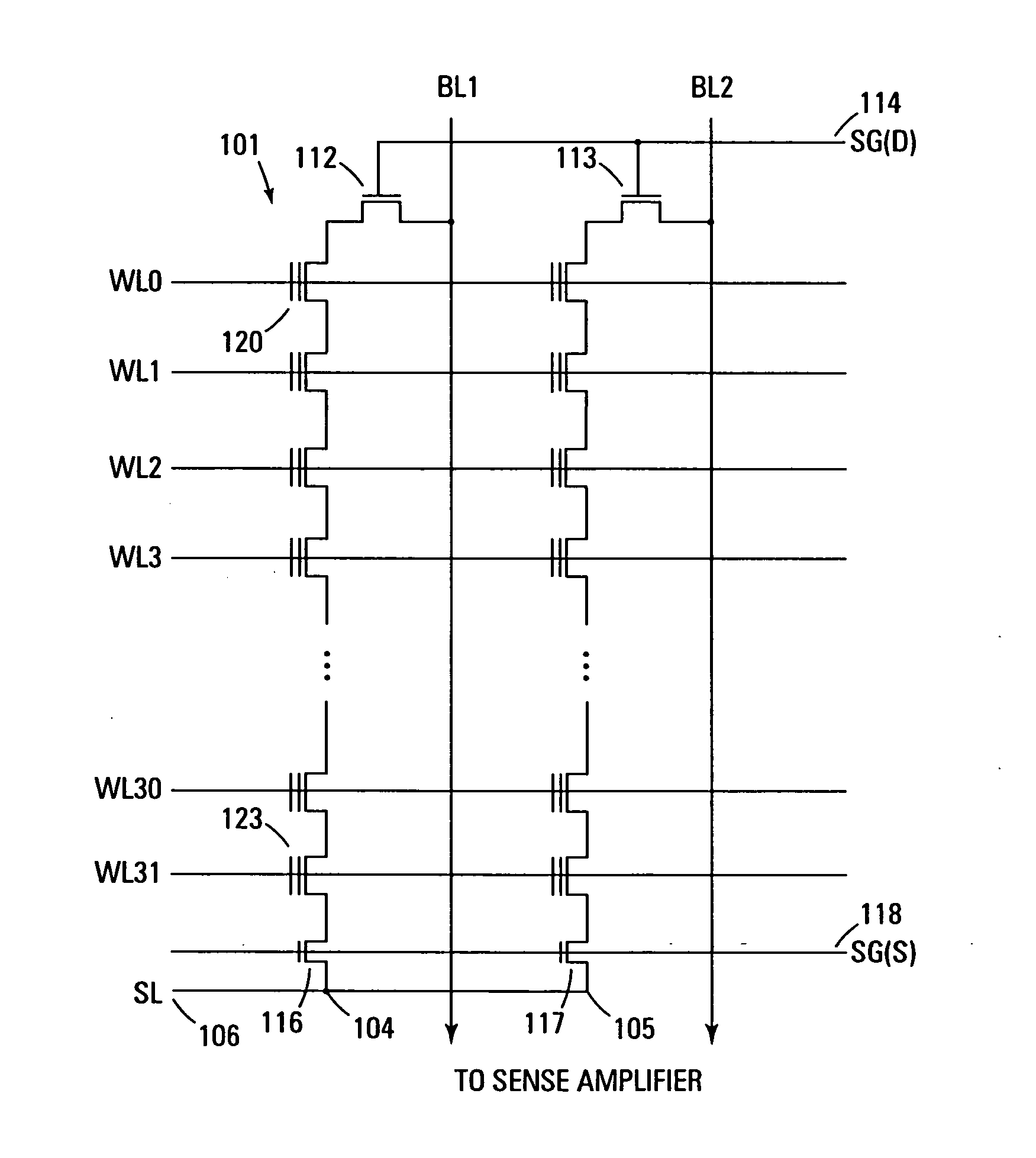
[0017]FIG. 1 illustrates a NAND flash array is comprised of an array of floating gate cells 101 arranged in series strings 104, 105. Each of the floating gate cells are coupled drain to source ...


PUM


Abstract

A non-volatile memory device has a plurality of memory cells that are organized into memory blocks. Each block can operate in either a multiple level cell mode or a single bit per cell mode. One dedicated memory block is capable of operating only in the single bit per cell mode. If the dedicated memory block is found to be defective, a defect-free block can be remapped to that dedicated memory block location to act only in the single bit per cell mode.

Description

TECHNICAL FIELD OF THE INVENTION [0001] The present invention relates generally to memory devices and in particular the present invention relates to non-volatile memory devices. BACKGROUND OF THE INVENTION [0002] Memory devices are typically provided as internal, semiconductor, integrated circuits in computers or other electronic devices. There are many different types of memory including random-access memory (RAM), read only memory (ROM), dynamic random access memory (DRAM), synchronous dynamic random access memory (SDRAM), and flash memory. [0003] Flash memory devices have developed into a popular source of non-volatile memory for a wide range of electronic applications. Flash memory devices typically use a one-transistor memory cell that allows for high memory densities, high reliability, and low power consumption. Common uses for flash memory include personal computers, personal digital assistants (PDAs), digital cameras, and cellular telephones. Program code and system data suc...

Claims


Application Information

Patent Timeline
IPC IPC(8): G11C11/34G11C11/56G11C16/04
CPCG11C11/5628G11C11/5642G06F11/1068G11C29/76G11C2211/5641G11C16/0483
Inventor ROOHPARVAR, FRANKIE F.
Owner ROUND ROCK RES LLC
Why Eureka
Try Eureka