Light emitting device with an integrated monitor photodiode

a technology of photodiodes and light emitting devices, which is applied in the direction of semiconductor lasers, laser details, electrical equipment, etc., can solve the problems of altering the optical characteristics of lasers and increasing costs, and achieve the effect of increasing the susceptibility of laser diodes to light reflection

Inactive Publication Date: 2005-12-29
II VI DELAWARE INC
View PDF12 Cites 44 Cited by
  • Summary
  • Abstract
  • Description
  • Claims
  • Application Information

AI Technical Summary

Benefits of technology

[0013] Some embodiments of the invention may include other features such as optimizations for use in self mixing applications. By increasing a laser diodes susceptibility to light reflections and by allowing laser wavelength to be controlled using a bias current, a self mixing optoelectronic device can be created. These devices may be used in creating various devices such us cursor pointers, imaging devices, linear measurement devices and the like.

Problems solved by technology

Various challenges exist when implementing a laser diode and photodiode together.
Using two discrete components, however, results in an increase of cost.
This however has the unfortunate drawback of causing the photodiode to become a part of the optics, particularly the mirror, of the laser thus altering the optical characteristics of the laser.

Method used


Image

  • Light emitting device with an integrated monitor photodiode
  • Light emitting device with an integrated monitor photodiode
  • Light emitting device with an integrated monitor photodiode

Examples


Embodiment Construction

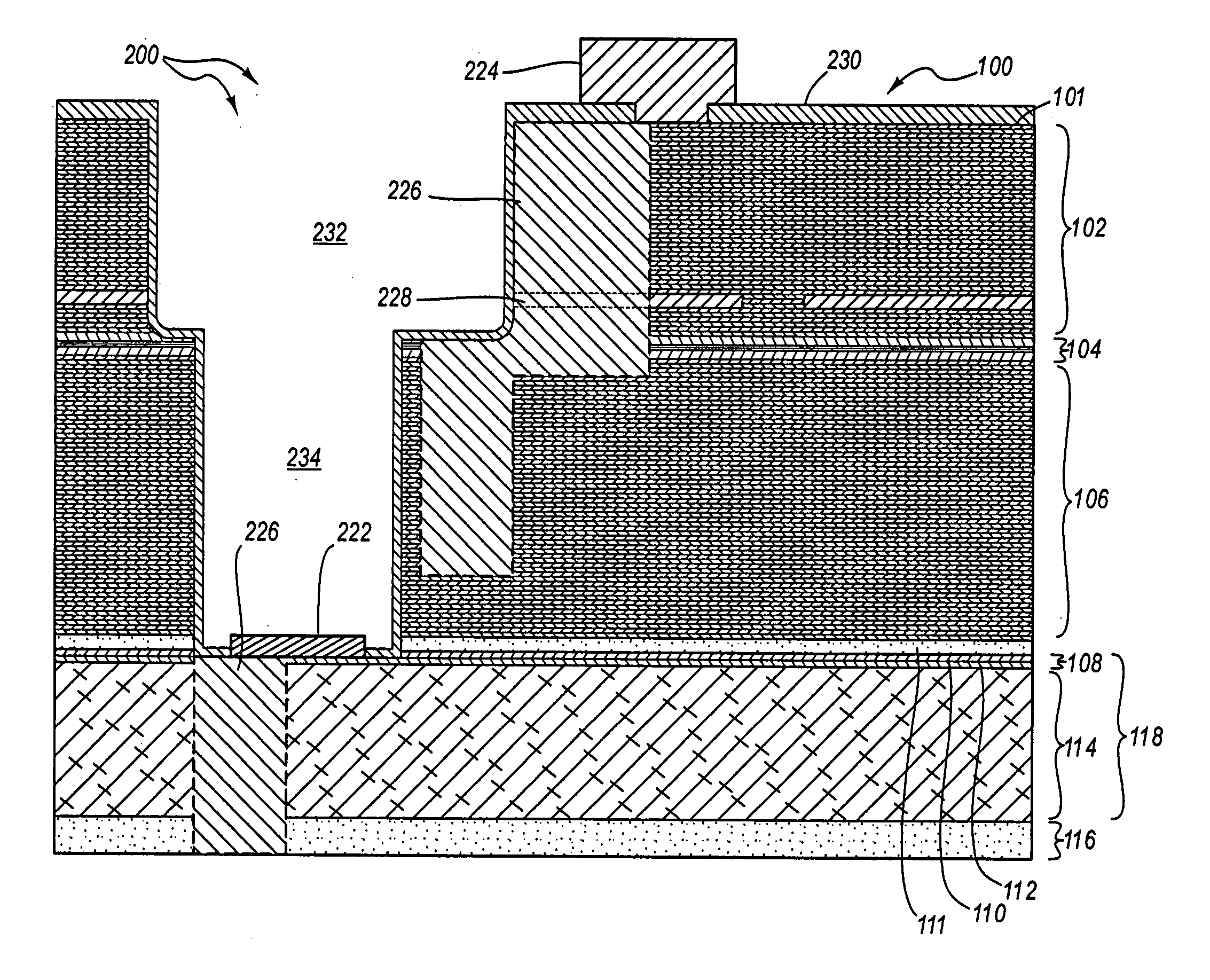
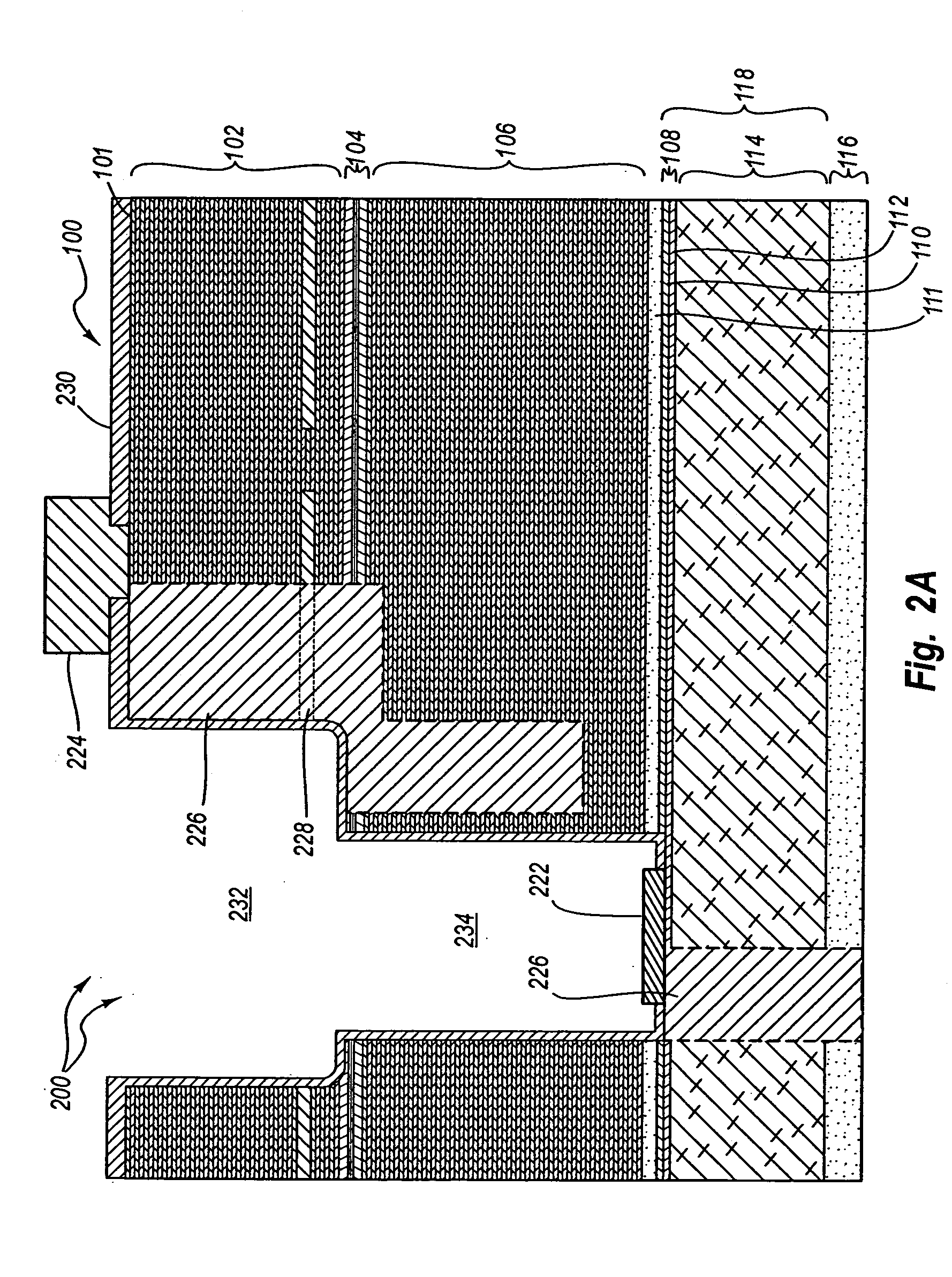
[0024] Some exemplary embodiments of the present invention include monolithically formed laser diodes and photodiodes. The laser diodes and photodiodes are connected through tunnel diodes such that a single power supply may be used to power the laser diodes and photodiodes. Appropriate contacts are formed to allow access to the various junctions of the laser diodes, tunnel diodes, and photodiodes.

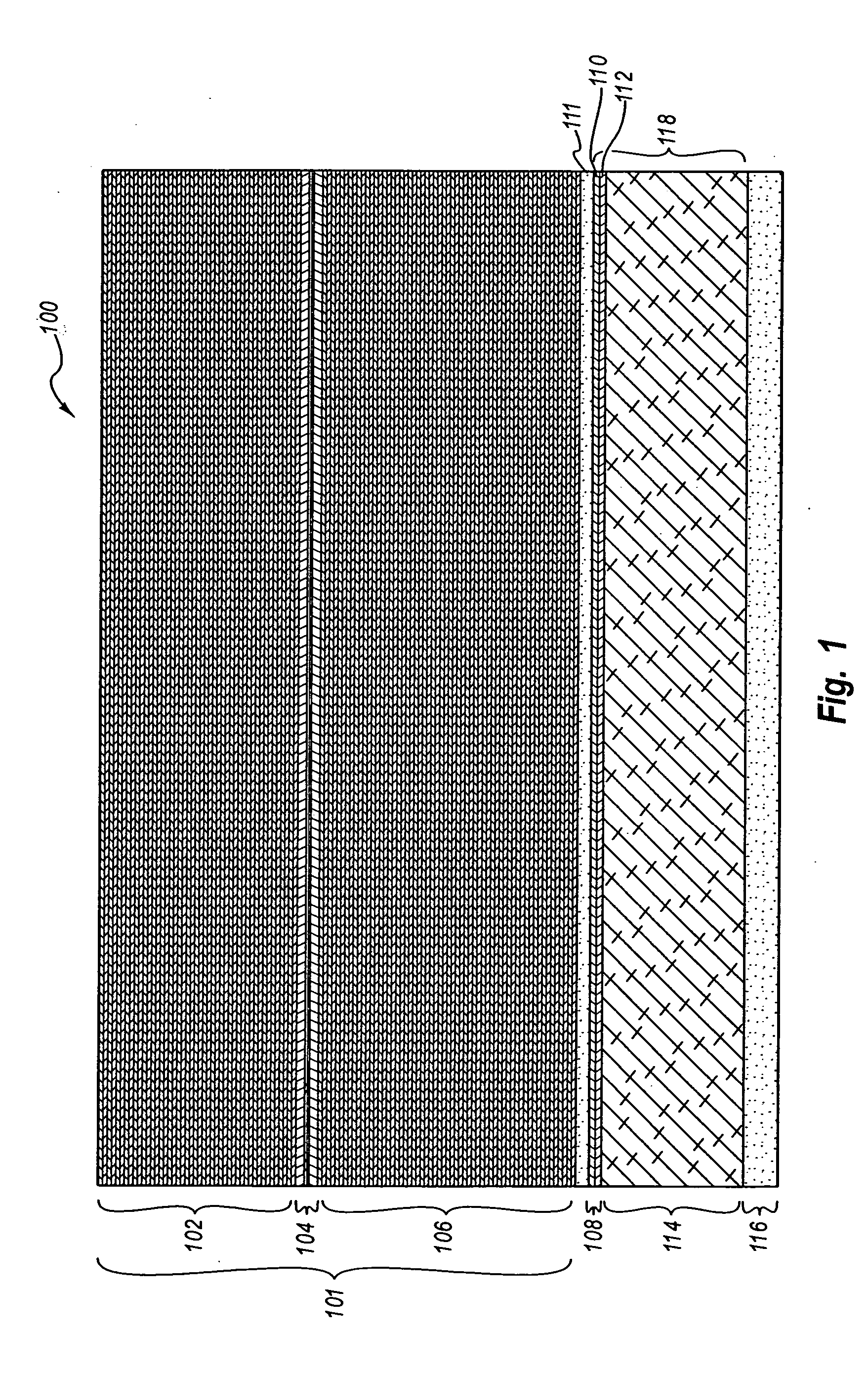
[0025] Referring now to FIG. 1, an example of an optoelectronic device including an epitaxial structure 100 that includes layers formed on a wafer substrate is shown. In one embodiment, the structure 100 is grown using a GaAs wafer. However, other III-V (three-five) semiconductor combinations may also be used. FIG. 1 shows a vertical cavity surface emitting laser (VCSEL) 101. The VCSEL 101 in the example shown includes a top mirror 102, an active region 104, and a bottom mirror 106. A PN junction exists in the active region 104.

[0026] A spacer layer 111 is formed below the bottom mirror 1...


PUM


Abstract

A monolithically formed laser and photodiode. The monolithically formed laser and photodiode includes a Vertical Cavity Surface Emitting Laser (VCSEL) that includes a first PN junction. The first PN junction includes a first p layer and a first n layer. A tunnel diode is connected to the VCSEL both physically and electronically through a wafer fabrication process. A photodiode is connected to the tunnel diode. The photodiode is connected to the tunnel diode by physical and electronic connections. The tunnel diode and photodiode may share some common layers. The tunnel diode includes a second PN junction. The monolithically formed laser and photodiode allow for an integrated structure with diode biasing flexibility including the use of a single supply to bias both the laser and photodiodes.

Description

BACKGROUND OF THE INVENTION [0001] 1. Field of the Invention [0002] The invention generally relates to vertical cavity surface emitting lasers. More specifically, the invention relates to using photodiodes in conjunction with vertical cavity surface emitting lasers. [0003] 2. Description of the Related Art [0004] Lasers have become useful devices with applications ranging from simple laser pointers that output a laser beam for directing attention, to high-speed modulated lasers useful for transmitting high-speed digital data over long distances. Several different types of lasers exist and find usefulness in applications at the present time. One type of laser is the edge emitter laser which is formed by cleaving a diode from a semiconductor wafer. Cleaving a diode from a semiconductor wafer forms mirrors that form a laser cavity defined by the edges of the laser diode. Edge emitter lasers may be designed to emit a laser beam more strongly from one of the edges than the other edges. H...

Claims


Application Information

Patent Timeline
Patent Type & Authority Applications(United States)
IPC IPC(8): H01S5/00H01S5/026H01S5/183
CPCH01S5/0264H01S5/18308H01S5/18313H01S5/1835H01S2301/02H01S5/2022H01S5/2027H01S5/3095H01S5/18358
Inventor GUENTER, JAMES
Owner II VI DELAWARE INC
Why Eureka
Try Eureka