Method of manufacturing a semiconductor device

a manufacturing method and semiconductor technology, applied in the direction of semiconductor devices, basic electric elements, electrical appliances, etc., can solve the problems of low response speed of devices, data stored therein may be lost with the lapse of time, and volatile semiconductor devices have a relatively high response speed, so as to improve electrical characteristics and reliability.

Inactive Publication Date: 2005-12-29
SAMSUNG ELECTRONICS CO LTD
View PDF11 Cites 25 Cited by
  • Summary
  • Abstract
  • Description
  • Claims
  • Application Information

AI Technical Summary

Benefits of technology

[0021] According to the present invention, no seam or void is generated in a polysilicon layer for a floating gate while the polysilicon layer is formed in a self-aligned process relative to an isolation layer formed on a substrate. Therefore, a semiconductor device including the polysilicon layer such as a flash memory device may have improved electrical characteristics and reliability.

Problems solved by technology

Volatile semiconductor devices have a relatively high response speed; however, data stored therein may be lost with the lapse of time.
Although non-volatile semiconductor devices permanently store data therein, such devices have a relatively low response speed.
However, due to decreasing design rules, the floating gates may not be precisely formed at the predetermined portions of the active region due to the active region's greatly reduced size.
However, poor step coverage may cause the polysilicon layer to not completely fill up the opening when the opening, thereby forming a seam in the polysilicon layer.
This seam formation problem is further exacerbated by the fact that openings formed through the isolation layer generally have an upper portion relatively narrower than a lower portion thereof.
This seam might not be completely removed in a subsequent process for forming a floating gate, therefore resulting in an undesired electrical effect.

Method used


Image

  • Method of manufacturing a semiconductor device
  • Method of manufacturing a semiconductor device
  • Method of manufacturing a semiconductor device

Examples


Embodiment Construction

[0026] The present invention now will be described more fully hereinafter with reference to the accompanying drawings, in which exemplary embodiments of the invention are shown. The present invention may, however, be embodied in many different forms and should not be construed as limited to the exemplary embodiments set forth herein; rather, these embodiments are provided so that this disclosure will be through and complete, and will fully convey the scope of the invention to those skilled in the art. In the drawings, the thickness of layers and regions are exaggerated for clarity. Like reference numerals refer to similar or identical elements throughout. It will be understood that when an element such as a layer, region or substrate is referred to as being “on” or “onto” another element, it can be directly on the other element or intervening elements may also be present.

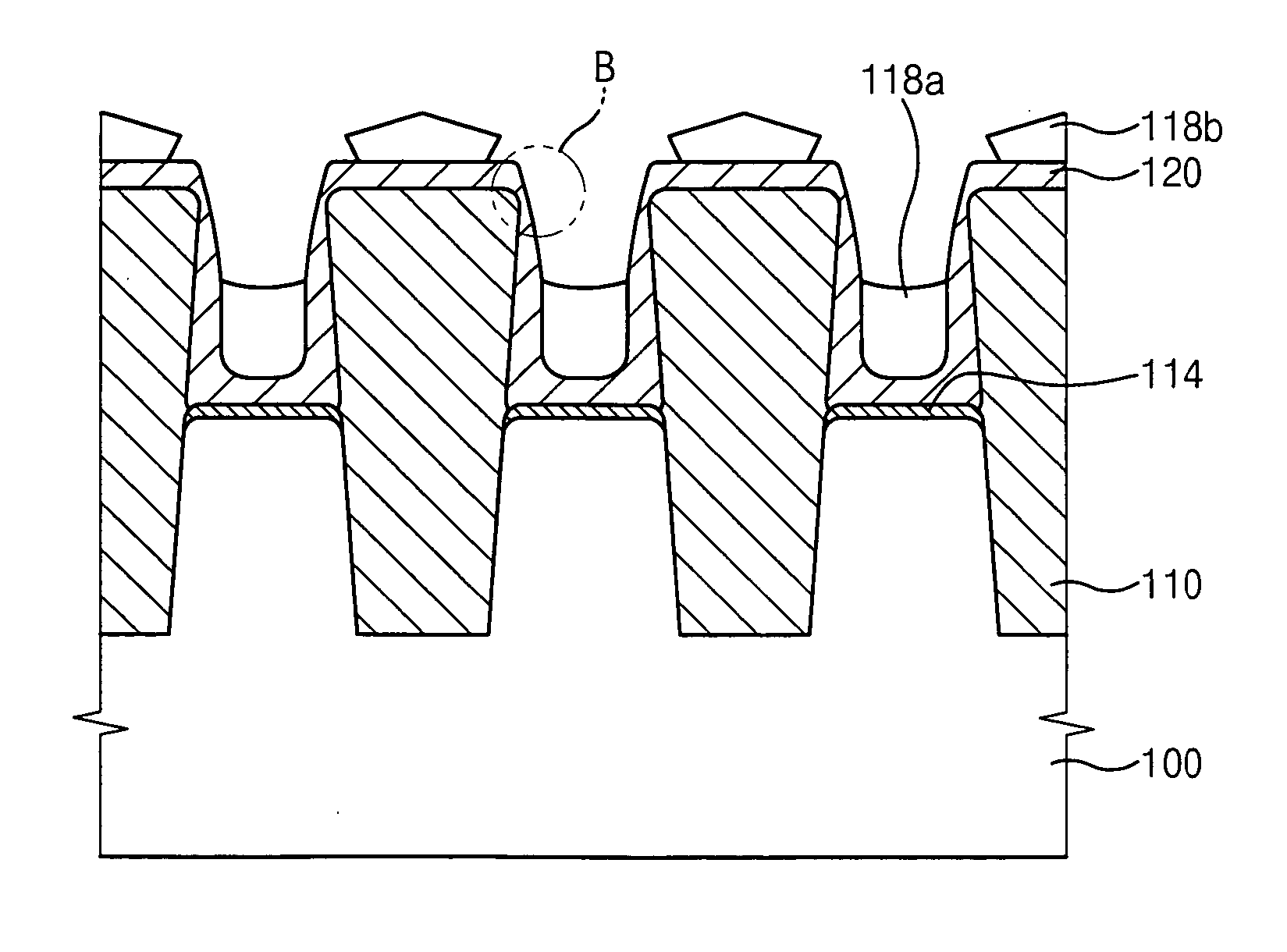
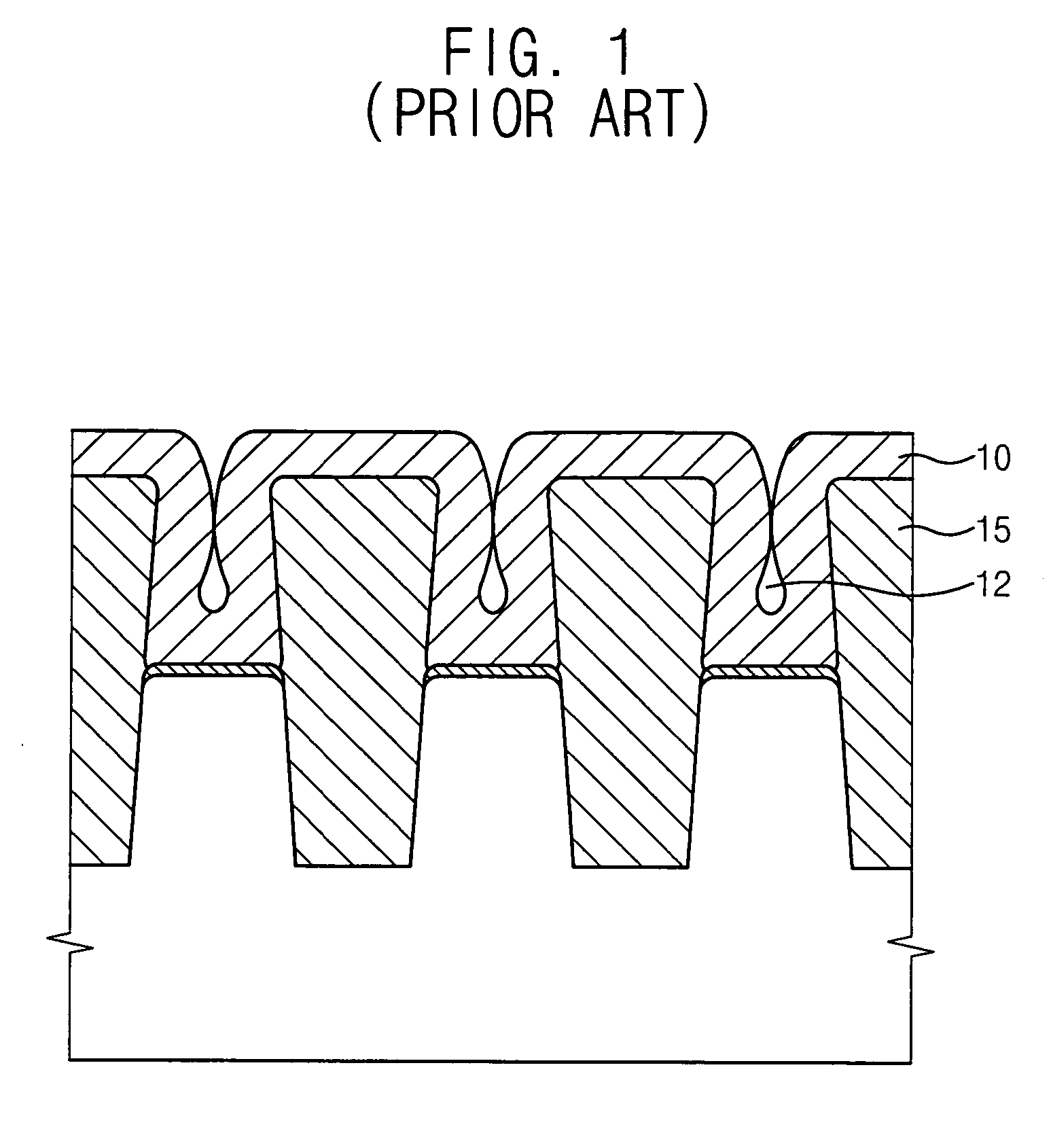
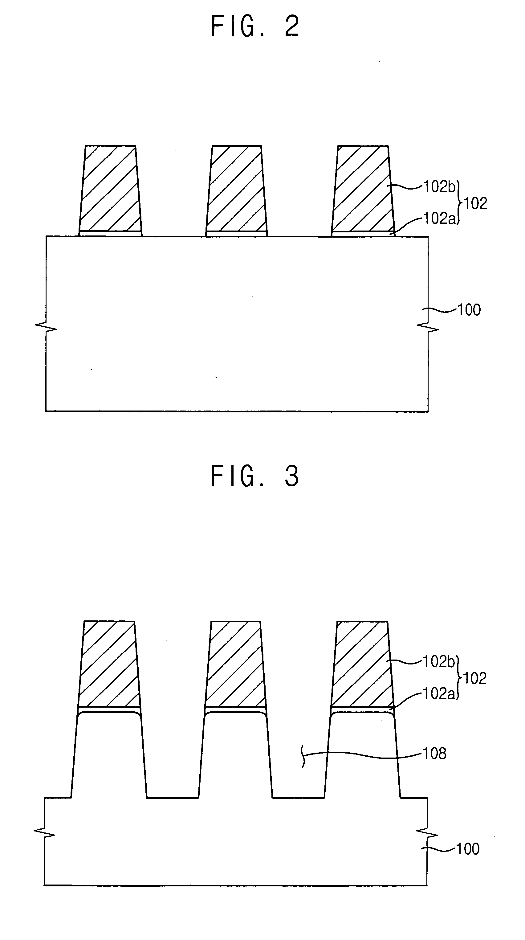
[0027] FIGS. 2 to 13 are cross sectional views illustrating a method of manufacturing a semiconductor device in ...


PUM


Abstract

In a method of manufacturing a semiconductor device, an isolation pattern is formed on a substrate. The isolation pattern includes an opening that exposes a portion of the substrate. A preliminary polysilicon layer is formed on the substrate and the isolation pattern to partially fill up the opening. A sacrificial layer is formed on the preliminary polysilicon layer. The sacrificial layer is partially etched to expose a portion of the preliminary polysilicon layer formed on a shoulder portion of the isolation pattern. A first polysilicon layer is formed by etching the exposed portion of the preliminary polysilicon layer to enlarge an upper width of the opening. After the etched sacrificial layer is removed, a second polysilicon layer is formed on the first polysilicon layer to fill up the enlarged opening. Because the upper width of the opening is larger than the lower width, no seam or void would be generated in the second polysilicon layer, therefore improving the electrical characteristics and reliability of the device.

Description

CROSS REFERENCE TO RELATED APPLICATIONS [0001] This application claims priority under 35 USC § 119 to a Korean Patent Application No. 2004-49250 filed on Jun. 29, 2004 the contents of which are incorporated herein by reference in their entirety. BACKGROUND OF THE INVENTION [0002] 1. Field of the Invention [0003] The present invention relates to a method of manufacturing a semiconductor device. More particularly, the present invention relates to a method of manufacturing a semiconductor device including a self-aligned polysilicon layer having no seam or void therein. [0004] 2. Description of the Related Art [0005] Semiconductor devices are generally divided into volatile semiconductor devices, such as dynamic random access memory (DRAM) devices or static random access memory (SRAM) devices, and non-volatile semiconductor devices like a read only memory (ROM) devices. Volatile semiconductor devices have a relatively high response speed; however, data stored therein may be lost with th...

Claims


Application Information

Patent Timeline
Patent Type & Authority Applications(United States)
IPC IPC(8): H01L21/76H01L21/762H01L21/763H01L21/8238H01L21/8247H01L27/115H01L29/76H01L29/94H01L31/062H01L31/113H01L31/119
CPCH01L21/76224H01L27/11521H01L27/115H01L21/763H10B69/00H10B41/30
Inventor KIM, TAEK-JUNGKIM, MIN
Owner SAMSUNG ELECTRONICS CO LTD
Why Eureka
Try Eureka