Film formation apparatus and method for semiconductor process

a film formation apparatus and semiconductor technology, applied in the direction of coatings, chemical vapor deposition coatings, electric discharge tubes, etc., can solve the problems of low throughput and low film formation rate of conventional film formation methods, and achieve high film quality and improve the effect of film formation ra

Active Publication Date: 2005-12-29
TOKYO ELECTRON LTD
View PDF3 Cites 126 Cited by
  • Summary
  • Abstract
  • Description
  • Claims
  • Application Information

AI Technical Summary

Benefits of technology

[0009] An object of the present invention is to provide a film formation method and film formation apparatus, which can greatly improve the film formation rate while maintaining a high film quality.

Problems solved by technology

However, conventional film formation methods of this kind can attain only a very low film formation rate and thus low throughput, in spite of plasma being used to promote the reaction.

Method used


Image

  • Film formation apparatus and method for semiconductor process
  • Film formation apparatus and method for semiconductor process
  • Film formation apparatus and method for semiconductor process

Examples


first embodiment

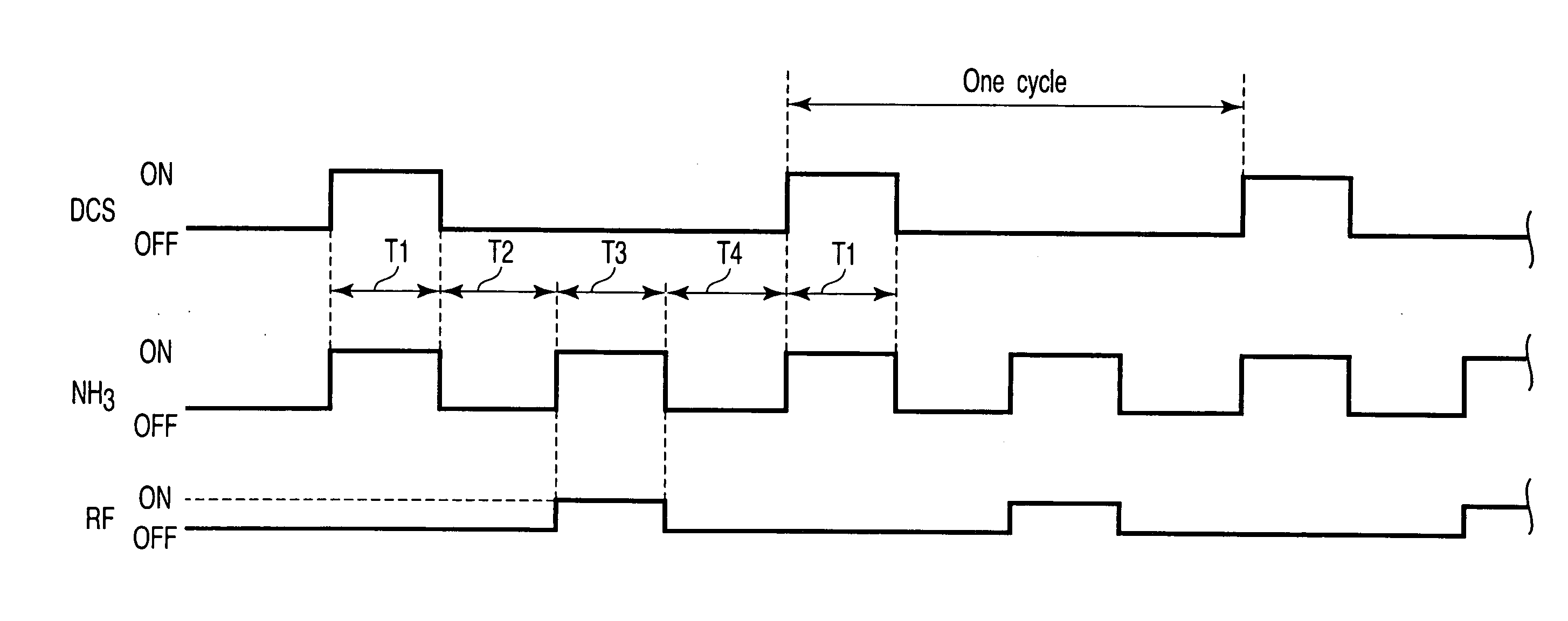
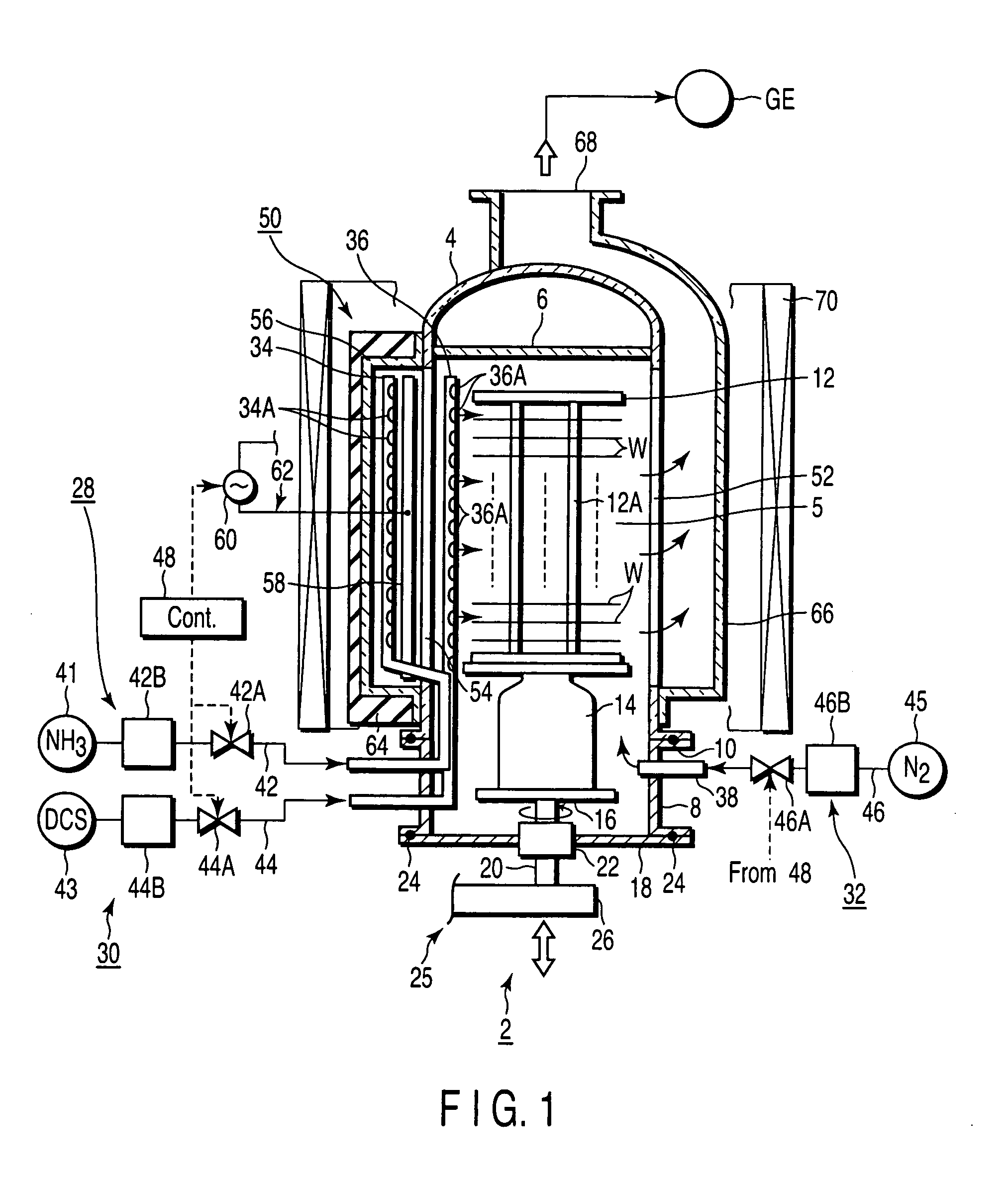
[0057]FIG. 1 is a sectional view showing a film formation apparatus (vertical CVD apparatus) according to a first embodiment of the present invention. FIG. 2 is a sectional plan view showing part of the apparatus shown in FIG. 1. The film formation apparatus 2 is arranged to supply a source gas (first process gas) and an assist gas (second process gas) to deposit a silicon nitride film (SiN), wherein the source gas contains dichlorosilane (DCS) gas as a silane family gas, and the assist gas contains ammonia (NH3) gas as a nitriding gas.

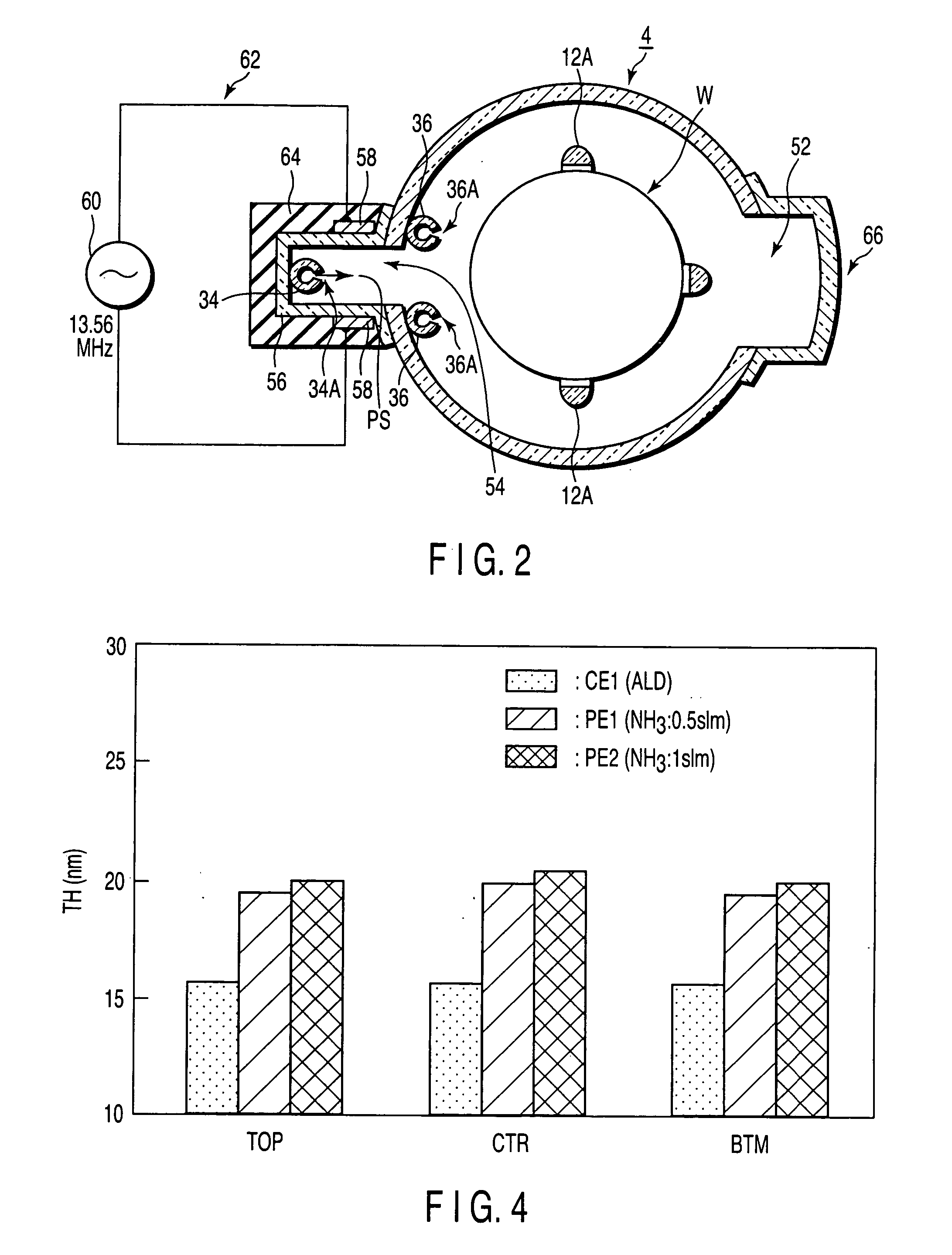
[0058] The apparatus 2 includes a process container 4 shaped as a cylindrical column with a ceiling and an opened bottom, in which a process field 5 is defined to accommodate and process a plurality of semiconductor wafers (target substrates) stacked at intervals. The entirety of the process container 4 is made of, e.g., quartz. The top of the process container 4 is provided with a quartz ceiling plate 6 to airtightly seal the top. The bottom of the ...

second embodiment

[0101]FIG. 9 is a sectional view showing a film formation apparatus (vertical CVD apparatus) according to a second embodiment of the present invention. The film formation apparatus 2X according to the second embodiment includes a supplementary gas supply circuit (third process gas supply circuit) 84 in addition to the assist gas supply circuit (second process gas supply circuit) 28, source gas supply circuit (first process gas supply circuit) 30, and purge gas supply circuit 32. The supplementary gas supply circuit 84 is arranged to supply a supplementary gas different from the source gas and assist gas. Specifically, the supplementary gas contains a gas selected from the group consisting of nitrogen gas, rare gas, nitrogen oxide gas, such as N2 or Ar gas used in this embodiment. The film formation apparatus 2X shown in FIG. 9 has essentially the same structure as the film formation apparatus 2 shown in FIG. 1 except for the portions relating to the supplementary gas supply circuit ...


PUM

PropertyMeasurementUnit
diameteraaaaaaaaaa
frequencyaaaaaaaaaa
frequencyaaaaaaaaaa

Abstract

A film formation method for a semiconductor process is arranged to form a thin film on a target substrate by CVD, while supplying a first process gas for film formation and a second process gas for reacting with the first process gas to a process field accommodating the target substrate. The method alternately includes first to fourth steps. The first step performs supply of the first and second process gases to the process field. The second step stops supply of the first and second process gases to the process field. The third step performs supply of the second process gas to the process field while stopping supply of the first process gas to the process field. The fourth step stops supply of the first and second process gases to the process field.

Description

CROSS-REFERENCE TO RELATED APPLICATIONS [0001] This application is based upon and claims the benefit of priority from prior Japanese Patent Applications No. 2004-190233, filed Jun. 28, 2004; and No. 2005-048059, filed Feb. 23, 2005, the entire contents of both of which are incorporated herein by reference. BACKGROUND OF THE INVENTION [0002] 1. Field of the Invention [0003] The present invention relates to a film formation apparatus and method for a semiconductor process for forming a thin film on a target substrate, such as a semiconductor wafer. The term “semiconductor process” used herein includes various kinds of processes which are performed to manufacture a semiconductor device or a structure having wiring layers, electrodes, and the like to be connected to a semiconductor device, on a target substrate, such as a semiconductor wafer or a glass substrate used for an LCD (Liquid Crystal Display) or FPD (Flat Panel Display), by forming semiconductor layers, insulating layers, and ...

Claims


Application Information

Patent Timeline
Patent Type & Authority Applications(United States)
IPC IPC(8): C23C16/34C23C16/452H01J37/32H01L21/20H01L21/314H01L21/318H01L21/36
CPCC23C16/345H01L21/0228C23C16/45523C23C16/45525C23C16/45527C23C16/45542C23C16/45546C23C16/45578H01J37/3244H01J2237/3321H01L21/3145H01L21/3185H01L21/0217H01L21/02211H01L21/02274C23C16/452H01L21/205H01L21/31
Inventor HASEBE, KAZUHIDECHOU, PAO-HWA
Owner TOKYO ELECTRON LTD
Why Eureka
Try Eureka