Method for manufacturing compound semiconductor wafer and compound semiconductor device

a semiconductor wafer and semiconductor technology, applied in the direction of semiconductor devices, electrical equipment, basic electric elements, etc., can solve the problem of difficult to control the carrier concentration to a desired valu

Inactive Publication Date: 2006-01-05
SUMITOMO CHEM CO LTD +1
View PDF2 Cites 5 Cited by
  • Summary
  • Abstract
  • Description
  • Claims
  • Application Information

AI Technical Summary

Benefits of technology

[0009] The object of the present invention is to provide a method for producing a compound semiconductor wafer and a compound semiconductor device which can solve the above problems in the conventional technologies.

Problems solved by technology

According to the above proposed conventional method, it is disclosed that the carrier concentration can be controlled to 1×1018 cm−3-1×1020 cm−3, but the method has a problem that when the feeding molar ratio of the raw material of Group V and that of Group III and the growth temperature are determined, the carrier concentration is determined thereby and thus it is difficult to control the carrier concentration to a desired value.

Method used


Image

  • Method for manufacturing compound semiconductor wafer and compound semiconductor device
  • Method for manufacturing compound semiconductor wafer and compound semiconductor device
  • Method for manufacturing compound semiconductor wafer and compound semiconductor device

Examples


example 1

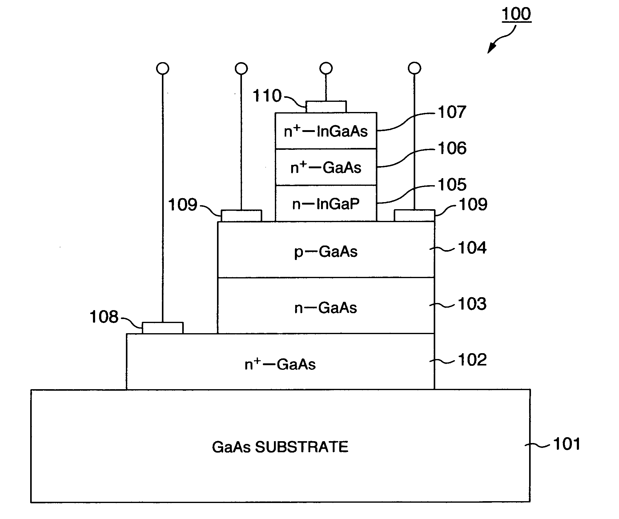
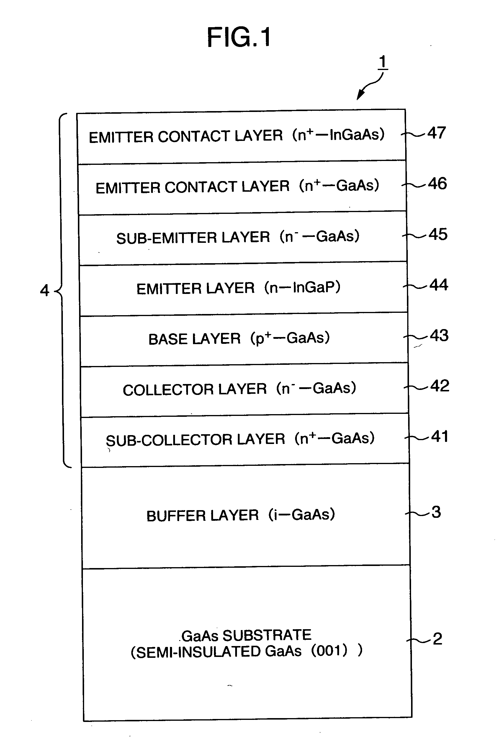
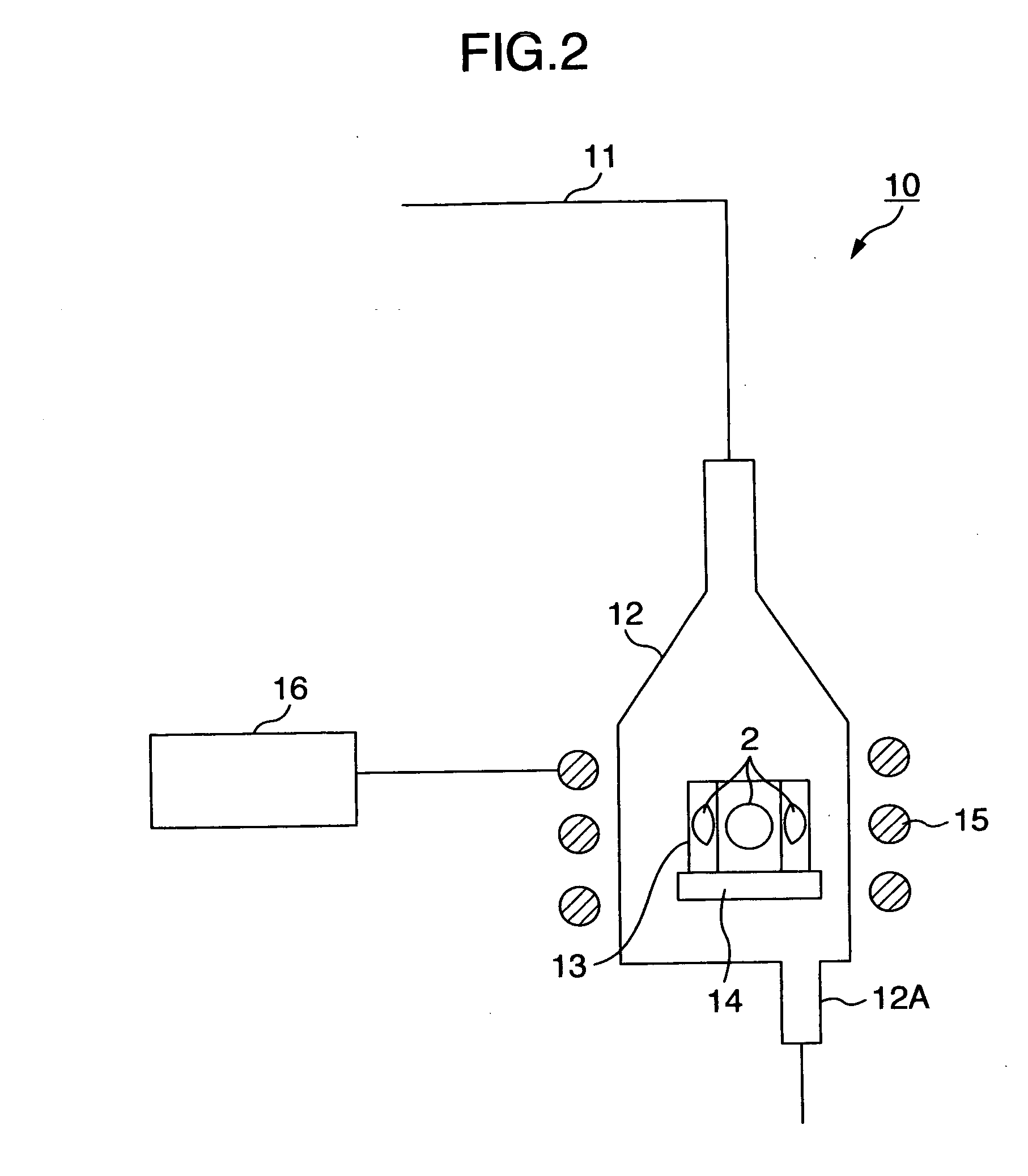
[0045] The growth conditions of base layer 43 were as follows. Growth temperature: 620° C.; raw material of Group III: trimethylgallium (TMG); raw material of Group V: arsine (AsH3); dopant for forming p-type base layer: CBrCl3; and V / III ratio: 0.9. Under the above growth conditions, the carrier concentration of the base layer 43 of 3.6×1019 cm−3 was obtained by adjusting the doping amount of C as a dopant. The current gain β of the HBT device in this case was measured to obtain 180. Further, a ratio of current gain β / base sheet resistance BRs was measured to obtain 0.60.

example 2

[0046] An HBT device was produced under the same conditions as in Example 1, except that the V / III ratio was 0.7, and the current gain β of the HBT device was measured to obtain 215. Further, the life time of minority carriers in the base layer 43 was measured to obtain 230 psec. The ratio of current gain β / base sheet resistance BRs was measured to obtain 0.70.


PUM


Abstract

A method for producing a compound semiconductor wafer used for production of HBT by vapor growth of a sub-collector layer, a collector layer, a base layer and an emitter layer in this turn on a compound semiconductor substrate using MOCVD method wherein the base layer is grown as a p-type compound semiconductor thin film layer containing at least one of Ga, Al and In as a Group III element and As as a Group V element under such growth conditions that the growth rate gives a growth determined by a Group V gas flow rate-feed.

Description

TECHNICAL FIELD [0001] The present invention relates to a method for producing a compound semiconductor wafer used for production of hetero junction bi-polar transistors (HBTs), and to a compound semiconductor device. BACKGROUND ART [0002] Hetero junction bi-polar transistors (HBTs) are bi-polar transistors in which an emitter-base junction is a hetero junction using a material greater in band gap than a base layer for an emitter layer in order to enhance the emitter injection efficiency, and since HBT is suitable as semiconductor devices used in the frequency area higher than microwave band, they are expected to be used as semiconductor devices for portable telephones of the next generation. [0003] The structure of HBT is as follows. In the case of, for example, a GaAs-based HBT, generally an n+-GaAs layer (sub-collector layer), an n-GaAs layer (collector layer), a p-GaAs layer (base layer), an n-InGaP layer (emitter layer) and an n-GaAs layer (sub-emitter layer) are in turn grown ...

Claims


Application Information

Patent Timeline
Patent Type & Authority Applications(United States)
IPC IPC(8): H01L29/47H01L21/336H01L29/739H01L21/331H01L29/74H01L21/205H01L29/737
CPCH01L21/02395H01L21/02463H01L21/02546H01L29/7371H01L21/0262H01L29/66318H01L21/02579H01L29/737H01L21/205
Inventor YAMADA, HISASHIFUKUHARA, NOBORU
Owner SUMITOMO CHEM CO LTD
Why Eureka
Try Eureka