Transparent conductor based pinned photodiode

a photodiode and transparent conductor technology, applied in the field of cmos imagers, can solve the problems of image lag, difficult using the conventional methods of implant engineering to create a pinned photodiode, and decrease the quantum efficiency of the cell, so as to improve the short wavelength light response and increase the quantum efficiency of the photosensor.

Active Publication Date: 2006-01-05
MICRON TECH INC
View PDF16 Cites 37 Cited by
  • Summary
  • Abstract
  • Description
  • Claims
  • Application Information

AI Technical Summary

Benefits of technology

[0015] The invention provides a pinned photodiode with improved short wavelength light response. In exemplary embodiments of the invention, a gate oxide is formed over a doped, buried region in a semiconductor substrate. A gate conductor is formed on top of the gate oxide. The gate conductor is transparent, and in one embodiment is a layer of indium-tin oxide. The transparent conductor can be biased to reduce the need for a surface dopant in creating a pinned photodiode region. The biasing of the transparent conductor produces a hole-rich accumulation region near the surface of the substrate. The gate conductor material permits a greater amount of charges from short wavelength light to be captured in the photo-sensing region in the substrate, and thereby increases the quantum efficiency of the photosensor.

Problems solved by technology

An incomplete transfer of charge results in image lag.
It is difficult using the conventional methods of implant engineering to create a pinned photodiode having these desired characteristics.
Either the process requires significant and challenging mask levels and implant conditions (which can be costly) or potential barriers and wells may develop in the photo-sensing area, decreasing the quantum efficiency of the cell.
Furthermore, as the size of pixel cells continues to decrease due to desired scaling, implant optimization becomes increasingly more difficult.

Method used


Image

  • Transparent conductor based pinned photodiode
  • Transparent conductor based pinned photodiode
  • Transparent conductor based pinned photodiode

Examples


Embodiment Construction

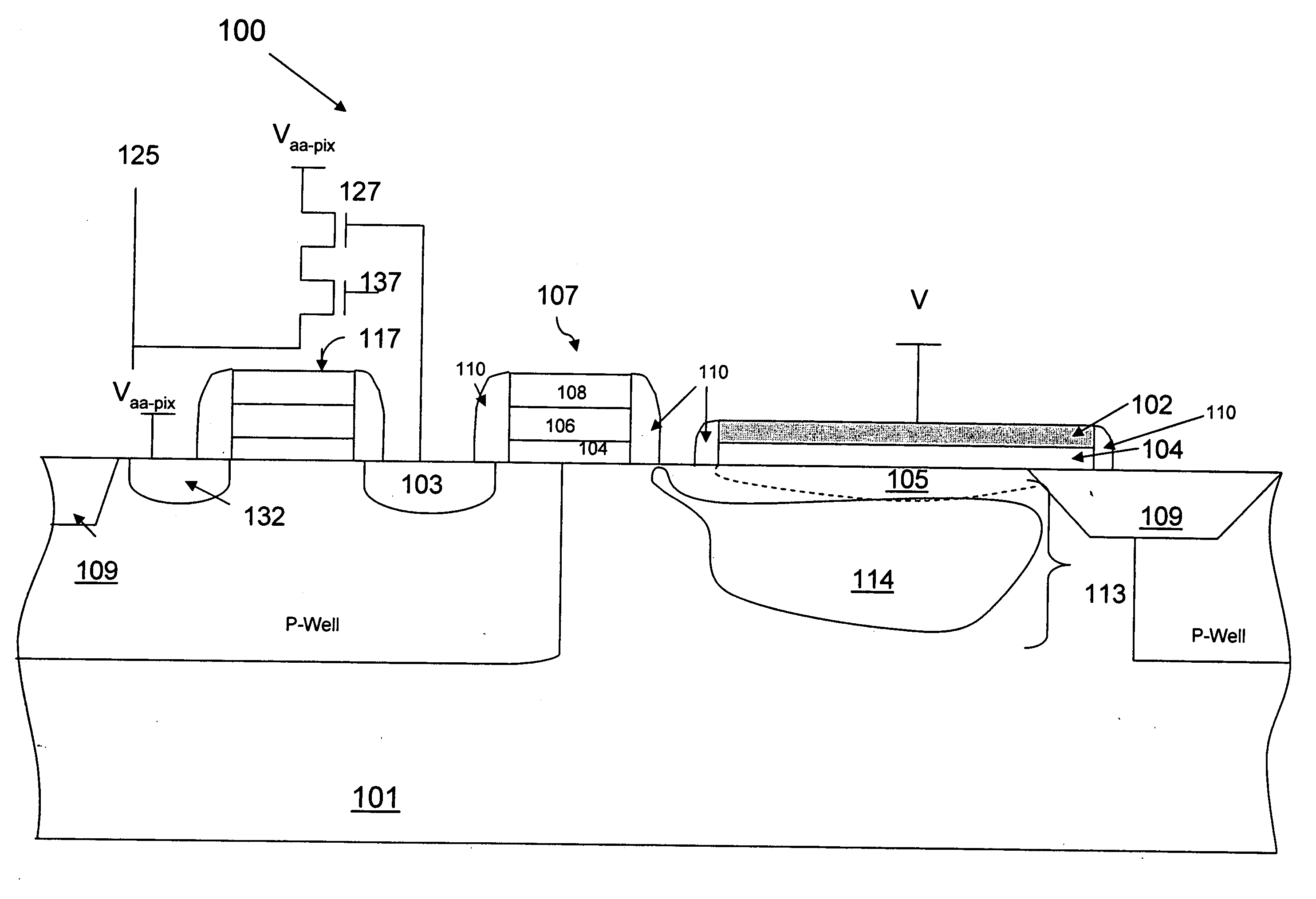
[0033] In the following detailed description, reference is made to the accompanying drawings which form a part hereof, and in which is shown by way of illustration specific embodiments in which the invention may be practiced. These embodiments are described in sufficient detail to enable those skilled in the art to practice the invention, and it is to be understood that other embodiments may be utilized, and that structural, logical and electrical changes may be made without departing from the spirit and scope of the present invention.

[0034] The terms “wafer” and “substrate” are to be understood as including silicon-on-insulator (SOI) or silicon-on-sapphire (SOS) technology, doped and undoped semiconductors, epitaxial layers of silicon supported by a base semiconductor foundation, and other semiconductor structures. Furthermore, when reference is made to a “wafer” or “substrate” in the following description, previous process steps may have been utilized to form regions or junctions...


PUM


Abstract

A pinned photodiode with improved short wavelength light response. In exemplary embodiments of the invention, a gate oxide is formed over a doped, buried region in a semiconductor substrate. A conductor is formed on top of the gate oxide. The gate conductor is transparent, and in one embodiment is a layer of indium-tin oxide. The transparent conductor can be biased to reduce the need for a surface dopant in creating a pinned photodiode region. The biasing of the transparent conductor produces a hole-rich accumulation region near the surface of the substrate. The gate conductor material permits a greater amount of charges from short wavelength light to be captured in the photo-sensing region in the substrate, and thereby increases the quantum efficiency of the photosensor.

Description

FIELD OF THE INVENTION [0001] The present invention relates generally to CMOS imagers and in particular to a CMOS imager having improved responsiveness to short wavelengths of light. BACKGROUND OF THE INVENTION [0002] CMOS imagers are increasingly being used as low cost imaging devices. A CMOS imager circuit includes a focal plane array of pixel cells, each one of the cells including a photosensor, for example, a photogate, photoconductor or a photodiode overlying a substrate for accumulating photo-generated charge in the underlying portion of the substrate. A readout circuit is connected to each pixel cell and includes at least pixel selecting field effect transistor formed in the substrate and a charge storage region formed on the substrate connected to the gate of a transistor coupled to the pixel selecting transistor. The charge storage region may be constructed as a floating diffusion region. The imager may include at least one electronic device such as a transistor for transfe...

Claims


Application Information

Patent Timeline
Patent Type & Authority Applications(United States)
IPC IPC(8): H01L31/062
CPCH01L27/14601H01L27/14689H01L27/1463H01L27/14609
Inventor MOULI, CHANDRARHODES, HOWARD E.
Owner MICRON TECH INC
Why Eureka
Try Eureka