Photogate with improved short wavelength response for a CMOS imager

a short wavelength response, photogate technology, applied in the field of cmos imagers, can solve the problems of high power dissipation of large arrays, ccd imagers also suffer from a number, and are susceptible to radiation damage, so as to improve the short wavelength light response and increase the quantum efficiency of the photosensor.

Inactive Publication Date: 2006-07-13
RHODES HOWARD E
View PDF42 Cites 4 Cited by
  • Summary
  • Abstract
  • Description
  • Claims
  • Application Information

AI Technical Summary

Benefits of technology

[0025] The present invention provides a photogate with improved short wavelength light response. A gate oxide is formed over a doped semiconductor substrate and a gate conductor is formed on top of the gate oxide. The gate conductor has a thickness within the range of approximately 50 to 1500 Angstroms, and is preferably approximately 50 to 800 Angstroms thick. Also provided is a stacked photogate having two layers: an upper transparent conductive layer formed of indium tin oxide, indium oxide, tin oxide, or other material, and a lower silicon layer with a thickness of approximately 50 to 800 Angstroms. Also provided is a photogate comprising a thin transparent conductive layer, approximately 100 to 3000 Angstroms thick, formed of indium tin oxide, indium oxide, tin oxide, or other material. The very thin photogate permits a greater amount of short wavelength light to pass through the photogate to reach the photosite in the substrate, and thereby increases the quantum efficiency of the photosensor.

Problems solved by technology

However, CCD imagers also suffer from a number of disadvantages.
For example, they are susceptible to radiation damage, they exhibit destructive read-out over time, they require good light shielding to avoid image smear and they have a high power dissipation for large arrays.
Additionally, while offering high performance, CCD arrays are difficult to integrate with CMOS processing in part due to a different processing technology and to their high capacitances, complicating the integration of on-chip drive sued signal processing electronics with the CCD array.
While there have been some attempts to integrate on-chip signal processing with CCD arrays, these attempts have not been entirely successful.
CCDs may also suffer from incomplete charge transfer from pixel to pixel which results in image smear.
A disadvantage of conventional photogates, however, is poor quantum efficiency for short wavelength light, i.e., wavelengths less than 500 nm, such as green, blue, or violet light.
Most prior art methods to solve the poor short wavelength efficiency of imagers have utilized photodiodes, and relatively few methods have been proposed for photogate-based imagers.
These methods add complexity to the manufacturing process of the imager, however, and have not succeeded in making photogates competitive with photodiodes when increased short wavelength sensitivity is desired.

Method used


Image

  • Photogate with improved short wavelength response for a CMOS imager
  • Photogate with improved short wavelength response for a CMOS imager
  • Photogate with improved short wavelength response for a CMOS imager

Examples


first embodiment

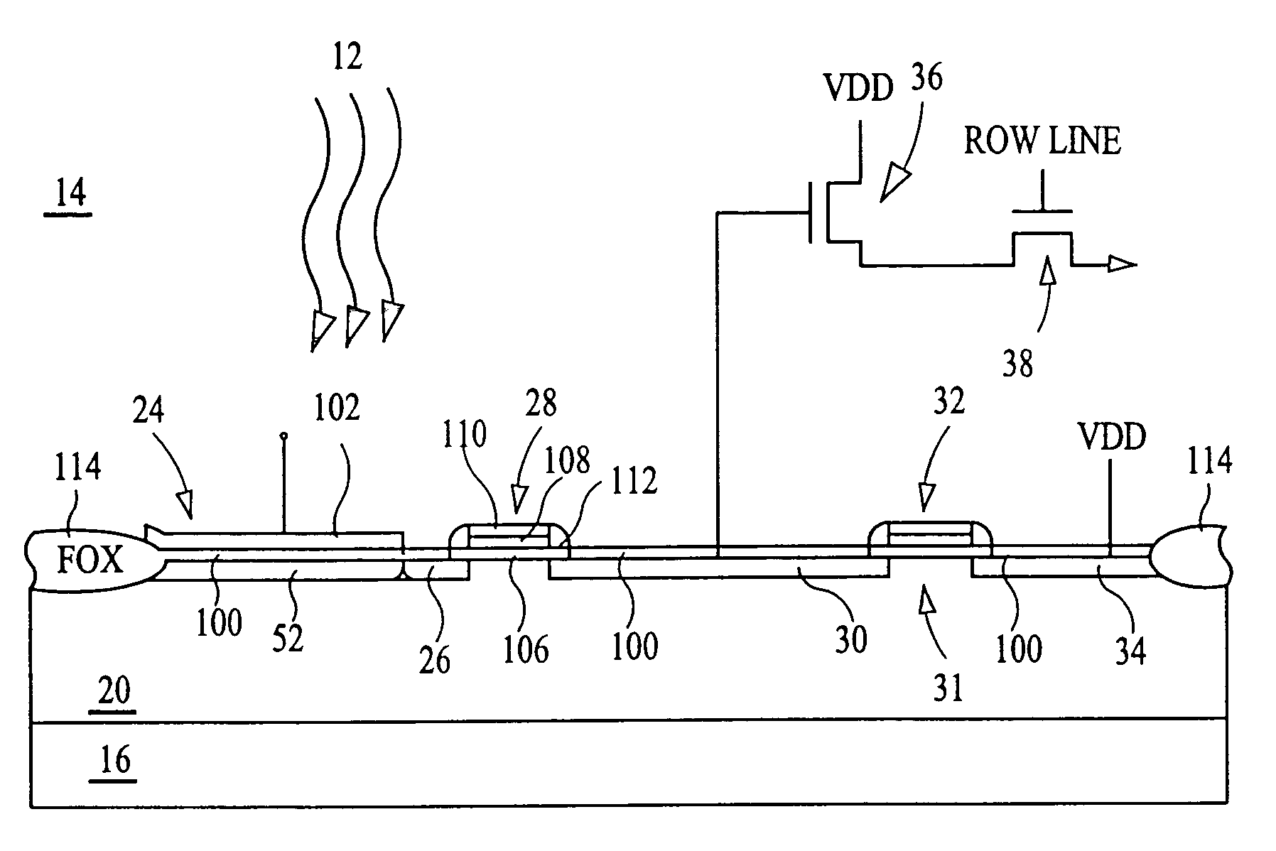
[0045] The structure of the pixel cell 14 of the first embodiment is shown in more detail in FIGS. 5 and 6. The pixel 14 may be formed in a substrate 16 having a doped layer or well 20 of a first conductivity type, which for exemplary purposes is treated as p-type. The doped layer 20 is provided with four doped regions 52, 26, 30, 34 formed therein, which are doped to a second conductivity type, which for exemplary purposes is treated as n-type. The first doped region 52 underlies the photogate 24, which comprises a thin layer 102 of doped silicon material transparent to radiant energy 12, such as doped polysilicon. The thin layer 102 is approximately 50 to 1500 Angstroms thick, and preferably has a thickness within the range of 50 to 800 Angstroms, and most preferably is 300 Angstroms thick.

[0046] A gate oxide layer 100 of silicon dioxide is formed between the thin layer 102 and the doped layer 20. Insulating sidewalls 112 of silicon dioxide (oxide), silicon nitride (nitride), sili...

second embodiment

[0058] The pixel cell 14 of the second embodiment requires further processing steps to form the photogate 24, as shown in FIG. 13. The top conductive latter 104 is formed by CVD or sputtering, or other suitable means, depending on the material of the layer 104. The layer 104 may be any transparent conductive material, such as indium tin oxide, indium oxide, tin oxide, or the like. The top conductive layer 104 is very thin, i.e., the thickness is within the range of 100 to 3000 Angstroms. After deposition of the layer 104, the layers 102 and 104 are patterned to form a stacked photogate 24. Conventional processing methods may then be used to form contacts and wiring to connect gate lines and other connections in the pixel cell 14, as described above.

[0059] The pixel cell 14 of the third embodiment is formed in a fashion similar to that of the first embodiment. After the pixel cell 14 has been processed up through the gate oxide formation depicted in FIG. 11, the next step is to form ...


PUM


Abstract

A photogate-based photosensor for use in a CMOS imager exhibiting improved short wavelength light response. The photogate is formed of a thin conductive layer about 50 to 3000 Angstroms thick. The conductive layer may be a silicon layer, a layer of indium and / or tin oxide, or may be a stack having an indium and / or tin oxide layer over a silicon layer. The thin conductive layer of the photogate permits a greater amount of short wavelength light to pass through the photogate to reach the photosite in the substrate, and thereby increases the quantum efficiency of the photosensor for short wavelengths of light.

Description

FIELD OF THE INVENTION [0001] The present invention relates generally to CMOS imagers and in particular to a CMOS imager having improved responsiveness to short wavelengths of light. BACKGROUND OF THE INVENTION [0002] There are a number of different types of semiconductor-based imagers, including charge coupled devices (CCDs), photodiode arrays, charge injection devices and hybrid focal plane arrays. CCD technology is often employed for image acquisition and enjoys a number of advantages which makes it the incumbent technology, particularly for small size imaging applications. CCDs are capable of large formats with small pixel size and they employ low noise charge domain processing techniques. [0003] However, CCD imagers also suffer from a number of disadvantages. For example, they are susceptible to radiation damage, they exhibit destructive read-out over time, they require good light shielding to avoid image smear and they have a high power dissipation for large arrays. Additional...

Claims


Application Information

Patent Timeline
Patent Type & Authority Applications(United States)
IPC IPC(8): H01L31/06H01L27/146H01L29/04H01L31/062H01L31/113
CPCH01L27/14601H01L27/14603H01L27/1462H01L27/1463H01L27/14643H01L27/14689
Inventor RHODES, HOWARD E.
Owner RHODES HOWARD E
Why Eureka
Try Eureka