

Solid-state imaging apparatus
- Summary
- Abstract
- Description
- Claims
- Application Information
AI Technical Summary
Benefits of technology
Problems solved by technology
Method used
Image

Examples
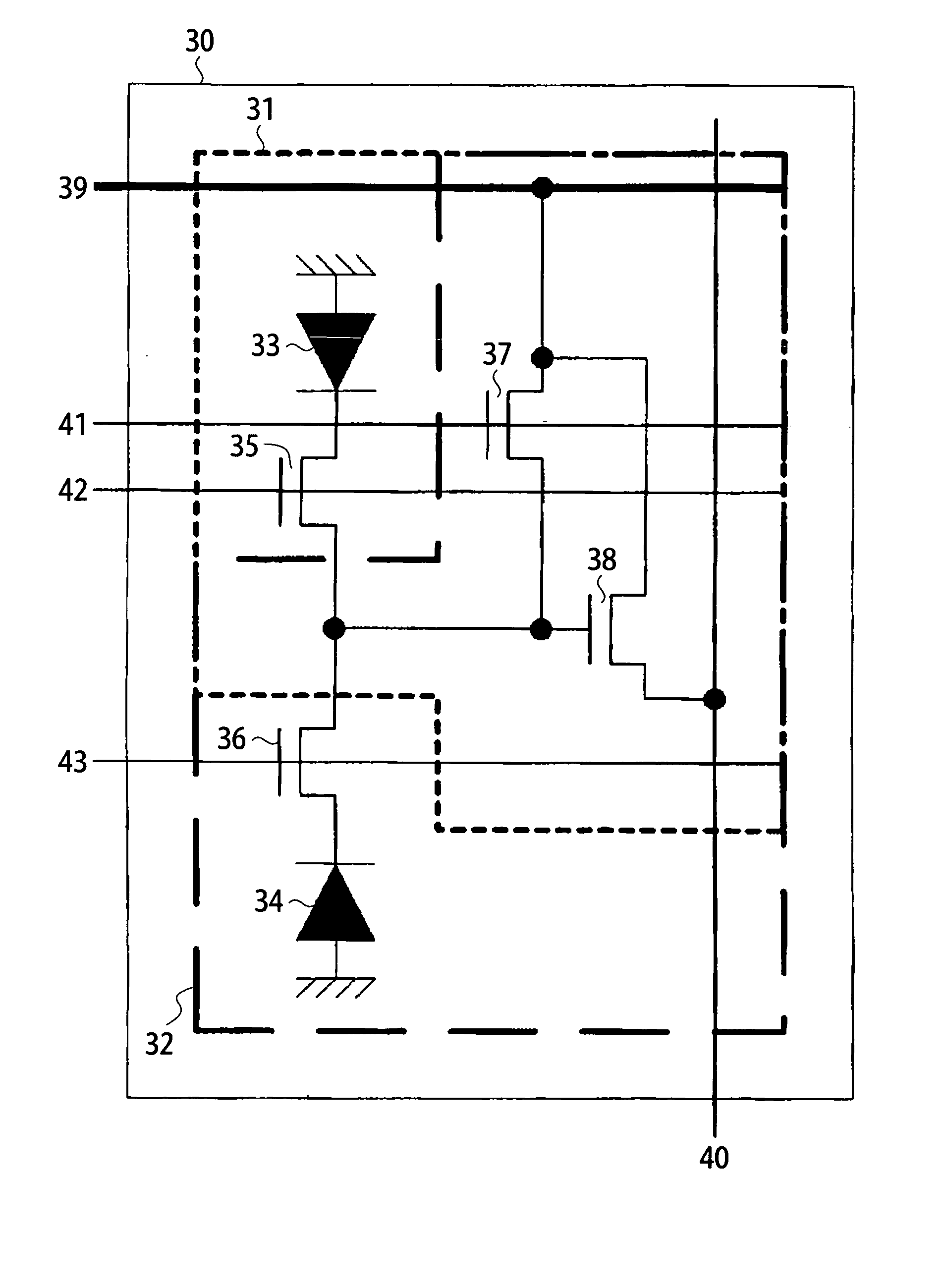
first embodiment
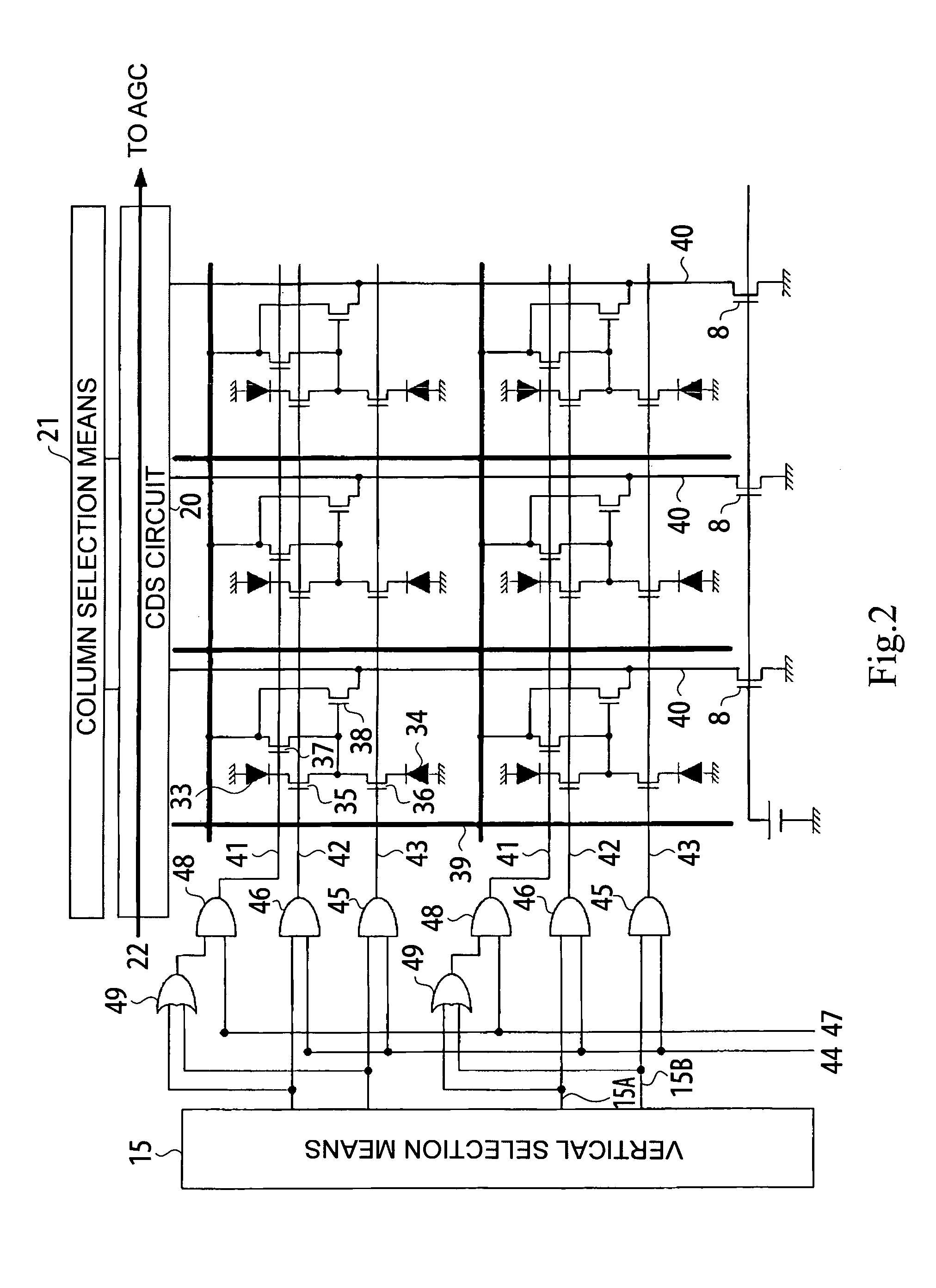
[0113] Sharing the transistors between the pixels and using the full-face signal line as one of the signal lines can greatly decrease the number of transistors and the number of signal lines for every pixel, thus possibly further reducing the pixel size.
second embodiment
[0114] The problem of sharing of the transistors between pixels, that is, the difference in the characteristics between the pixels filtered in the same color, which difference is caused by the use of pixels having different shapes, can be resolved by changing the arrangement of the unit cells to give the same shape to all the pixels filtered in the same color.
[0115] Although the case in which the unit cells, including the two vertically adjoining pixels sharing the transistors, are vertically shifted from each other by one pixel for every column in the imaging surface filtered in the Bayer format is exemplified, the method of devising the arrangement of the unit cells to give the same shape to the pixels filtered in the same color is applicable to other color filtering methods and other pixel structures. Furthermore, depending on the structure, shifting the unit cells by an amount smaller than one pixel is possibly preferable to shifting them by just one pixel.
third embodiment
[0116] When the signals are read out from the pixels in the imaging surface filtered in the Bayer format through the two divided output systems, the pixels filtered in the same color (the G pixels in the RG lines and the G pixels in the GB lines) are read out through the different output systems in a normal pixel structure. As a result, the variation in the characteristics between the output systems can result in horizontal stripes. The same problem is caused in the case in which the two vertically adjoining pixels share the transistors. In contrast, according to the third embodiment, sharing the transistors between the two diagonally adjoining pixels allows the outputs from the Gr pixels and Gb pixels to be read out through the same output system. Hence, the structure according to the third embodiment is not affected by any variation in the process occurring between the output systems and, therefore, it is possible to sample the images at double speed, compared with the cases using...
PUM
 Abstract
Description
Claims
Application Information