Liquid crystal display device and fabricating method thereof

a technology of liquid crystal display and display device, which is applied in the direction of instruments, non-linear optics, optics, etc., can solve the problems difficulty in increasing the height of inorganic insulating film, adhesive strength deterioration, etc., to improve the reliability of liquid crystal display, reduce the risk of liquid crystal contamination, and improve the adhesive strength of sealant

Inactive Publication Date: 2006-01-05
LG DISPLAY CO LTD
View PDF6 Cites 45 Cited by
  • Summary
  • Abstract
  • Description
  • Claims
  • Application Information

AI Technical Summary

Benefits of technology

[0015] An advantage of the present invention is that it reduces the risk of contamination of a liquid crystal material.
[0016] Another advantage of the present invention is that it improves liquid crystal display reliability by improving the adhesive strength of the sealant used to bond the two substrates forming the liquid crystal display device.
[0017] Additional advantages of the invention will be set forth in the description which follows, and in part will be apparent from the description, or may be learned by practice of the invention. The advantages of the invention will be realized and attained by the structure particularly pointed out in the written description and claims hereof as well as the appended drawings.
[0018] The aforementioned and other advantages of the present invention are achieved with a liquid crystal display device, which comprises a first and a second substrate having a liquid crystal region, a sealant region, and an outer region; a wiring disposed on the first substrate, the wiring crossing the sealant region; a gate insulating film disposed on the wiring; an organic insulating film disposed on a portion o

Problems solved by technology

Accordingly, it has a disadvantage in that it is difficult to increase the height of the inorganic insulating film.
The organic insulating film and the sealant, which is generally an epoxy resin have a weak adhesive characteristic such that its adhesive strength deteriorates over time.
Deterioration of the organic insulating film provides a path through which the moisture of the outside penetrates due to

Method used


Image

  • Liquid crystal display device and fabricating method thereof
  • Liquid crystal display device and fabricating method thereof
  • Liquid crystal display device and fabricating method thereof

Examples


first embodiment

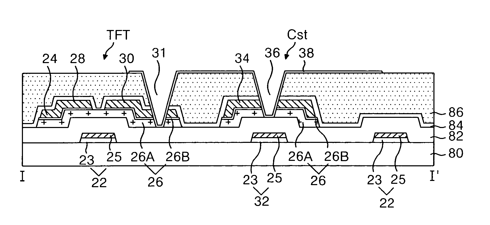
[0091]FIG. 11 is an enlarged plane view partially illustrating a sealing area of a thin film transistor substrate according to the present invention, and FIGS. 12A-12G are sectional diagrams illustrating a sealing area and a surrounding part thereof shown in FIG. 11, respectively taken along the lines V-V′, VI-VI′, VIIa-VIIa′, VIIb-VIIb′, VIIc-VIIc′, VIId-VIId′, VIIe-VIIe′;

[0092] The foregoing first wiring structure and wiring gap structure are applied to the seal area illustrated in FIGS. 11 and 12A-12G. Sectional view V-V′ in FIG. 12A and sectional view VI-VI′ in FIG. 12B illustrate a wiring part vertical structure and a wiring gap vertical structure taken in a wiring direction. Referring to FIGS. 12C-12G, sectional view VIIa-VIIa′, VIIb-VIIb′, VIIc-VIIc′, VIId-VIId′ and VIIe-VIIe′ respectively illustrate a cell inner part where the organic insulating film 86 exists; the cell inner part where the organic insulating film 86 is removed; the seal area where the organic insulating fil...

second embodiment

[0111] The seal area according to the present invention having such a structure is formed by four mask processes as shown in FIGS. 19A to 22H. The four mask processes are substantially similar to the four mask processes described above with reference to FIGS. 4A to 7B, thus it will be described in brief.

[0112] Referring to FIGS. 19A and 19H, there is formed a wiring of double structure such as the gate link 48, the data link 58 and the common link on the substrate 80 by a first mask process.

[0113] Referring to FIGS. 20A and 20B20H, the gate insulating film 82 is formed, which commonly covers the wirings. Also formed are the first and second dummy patterns 92, 93, which act as the etch stopper, to overlap each wiring together with the semiconductor pattern 26 underneath. Herein, the first dummy pattern 92 is formed along the wiring to the part of the seal area from the cell inner part which is adjacent to the seal area, and the second dummy pattern 93 integrated with the first dummy...


PUM


Abstract

The present invention provides a liquid crystal display panel that is adaptive for preventing a liquid crystal contamination as well as improving an adhesive strength of a sealant and an organic insulating film, and a fabricating method thereof. A liquid crystal display device according to an embodiment of the present invention includes: a first and a second substrate having a liquid crystal region, a sealant region, and an outer region; a wiring disposed on the first substrate, the wiring crossing the sealant region; a gate insulating film disposed on the wiring; an organic insulating film disposed on a portion of the wiring; and a sealant disposed on the sealant region of the first and second substrates, wherein the sealant is in contact with the gate insulating film.

Description

[0001] This application claims the benefit of the Korean Patent Application No. P2004-49954 filed on Jun. 30, 2004, which is hereby incorporated by reference. BACKGROUND OF THE INVENTION [0002] 1. Field of the Invention [0003] The present invention relates to a liquid crystal display panel having an organic insulating film. More particularly, the present invention relates to a liquid crystal display panel that is adaptive for preventing liquid crystal contamination as well as improving an adhesive strength of a sealant and an organic insulating film, and a fabricating method thereof. [0004] 2. Description of the Related Art [0005] A liquid crystal display device displays a picture by controlling the transmission of light through a liquid crystal by use of an electric field. A liquid crystal display device includes a liquid crystal display panel in which liquid crystal cells are arranged in a matrix shape, and a drive circuit to drive the liquid crystal display panel. [0006] The liqu...

Claims


Application Information

Patent Timeline
IPC IPC(8): G02F1/136
CPCG02F1/133345G02F1/136286G02F1/1345G02F1/1339
Inventor AHN, BYUNG CHUL
Owner LG DISPLAY CO LTD
Why Eureka
Try Eureka