Method for fabricating CMOS image sensor

Active Publication Date: 2006-01-05
TAIWAN SEMICON MFG CO LTD
View PDF21 Cites 21 Cited by
  • Summary
  • Abstract
  • Description
  • Claims
  • Application Information

AI Technical Summary

Benefits of technology

[0024] An object of the present invention is to provide a method for fabricating a CMOS image sensor, to decrease a dark current.
[0025] Another object of the present invention is to provi

Problems solved by technology

With the demands for a technology of the CMOS image sensor below 0.18 μm, the CMOS image sensor has the various problems in fabrication of pixel array, for example, the limit in size of pixel, the non-silicide process, and the uniformity of color filter array.
The silicide blocking layer 15a of the tapered edge profile has the problem in that it can not perform the blocking function in the silicide process.
H

Method used


Image

  • Method for fabricating CMOS image sensor
  • Method for fabricating CMOS image sensor
  • Method for fabricating CMOS image sensor

Examples


Example

[0040] Reference will now be made in detail to the preferred embodiments of the present invention, examples of which are illustrated in the accompanying drawings. Wherever possible, the same reference numbers will be used throughout the drawings to refer to the same or like parts.

[0041] Hereinafter, a method for fabricating a CMOS image sensor according to the present invention will be described with reference to the accompanying drawings.

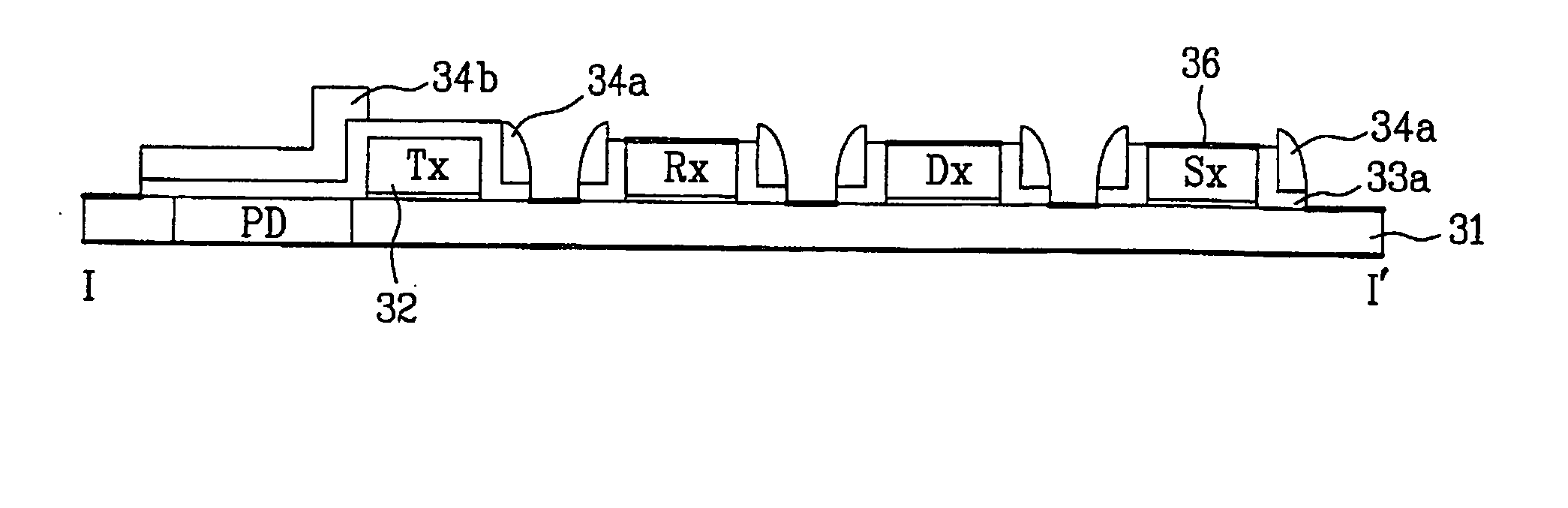
[0042]FIG. 7A and FIG. 7D are cross sectional views of showing the process for fabricating a CMOS image sensor according to the preferred embodiment of the present invention, which mainly show a photodiode PD and an adjacent transfer transistor Tx.

[0043] As shown in FIG. 7A, a photodiode area PD is formed in a semiconductor substrate 31, and then a plurality of gates are formed on the semiconductor substrate 31 by interposing a gate oxide layer. Among the plurality of gates, one side of the gate 32 of the transfer transistor Tx is aligned to the...


PUM


Abstract

A method for fabricating a CMOS image sensor is disclosed, to decrease a dark current, which includes the steps of forming a photodiode area in a semiconductor substrate; forming a plurality of gates including a first gate on the semiconductor substrate, wherein the first gate has one side aligned to the edge of the photodiode area; sequentially forming a first insulating layer and a second insulating layer on an entire surface of the semiconductor substrate; forming a first photoresist, wherein the firs photoresist is patterned so as to expose the upper side of the first gate and the other side of the gate being opposite to one side of the gate; forming a spacer at the other side of the first gate by dry-etching the second insulating layer in state of using the first photoresist as a mask, and forming a silicide blocking layer above the photodiode area; and removing the first photoresist.

Description

CROSS-REFERENCE TO RELATED APPLICATIONS [0001] This application claims the benefit of Korean Application No. P2004-51216 filed on Jul. 1, 2004, which is hereby incorporated by reference as if fully set forth herein. BACKGROUND OF THE INVENTION [0002] 1. Field of the Invention [0003] The present invention relates to an image sensor, and more particularly, to a method for fabricating a CMOS image sensor suitable for decreasing a dark current. [0004] 2. Discussion of the Related Art [0005] Generally, a CMOS image sensor is suitable for a SoC (System on Chip). As the CMOS image sensor is scaled down to a deep sub micron below 0.18 μm, the CMOS image sensor has more competitive power than CCD. [0006] With the demands for a technology of the CMOS image sensor below 0.18 μm, the CMOS image sensor has the various problems in fabrication of pixel array, for example, the limit in size of pixel, the non-silicide process, and the uniformity of color filter array. [0007] Among the various proble...

Claims


Application Information

Patent Timeline
IPC IPC(8): H01L21/8238
CPCH01L27/14689H01L27/14609H01L27/146H01L31/10
Inventor JANG, JAMES
Owner TAIWAN SEMICON MFG CO LTD
Why Eureka
Try Eureka