Memory element and memory device

a memory element and memory technology, applied in thermoelectric devices, instruments, nanoinformatics, etc., can solve the problems of cross-talk, large consumption power, and left-over memory high density,

Inactive Publication Date: 2006-01-12
SONY CORP
View PDF6 Cites 19 Cited by
  • Summary
  • Abstract
  • Description
  • Claims
  • Application Information

AI Technical Summary

Problems solved by technology

However, for practical use of the MRAM, problems caused along with high density of memories have been left.
Therefore, when a memory cell is miniaturized, a consumption power becomes very large.
Further, there is a risk that cross talk may be caused by a proximate leakage magnetic field between adjacent cells.
However, in this technique, there has been also a problem for practical use.
However, when the foregoing material is used for the paramagnetic layer, it is difficult to grow a uniform thin film, and to control the spin coherence length.
Therefore, there has been a problem that a sufficient spin coherence length and a uniform spin field cannot be obtained in the paramagnetic layer.
In the result, regarding the memory element of the spin injection method, though it is theoretically shown that significant effects can be obtained compared to the conventional induced magnetic field method, sufficient characteristics have not been obtained practically.
Therefore, its practical use has not been attained.

Method used


Image

  • Memory element and memory device
  • Memory element and memory device
  • Memory element and memory device

Examples


first embodiment

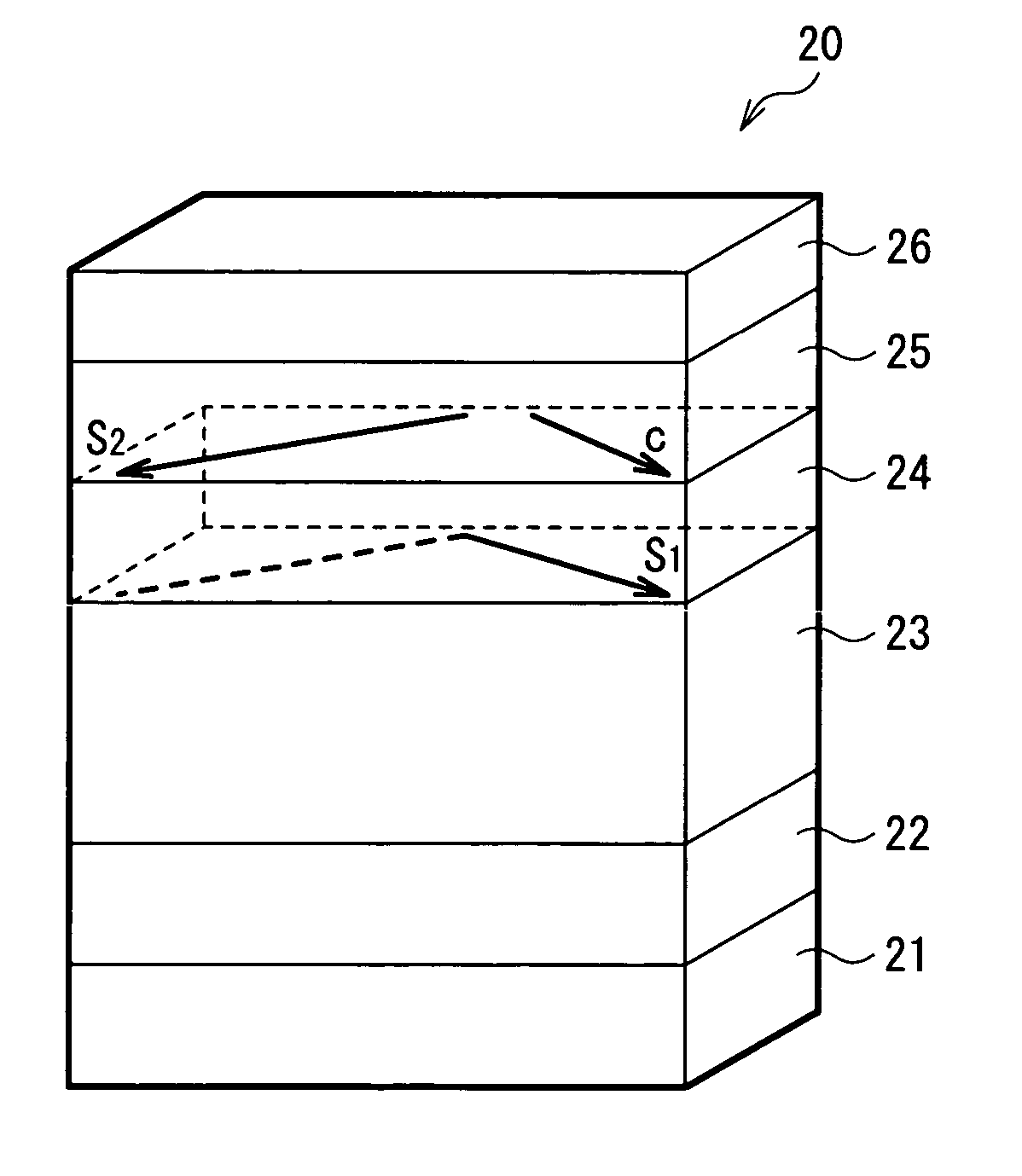
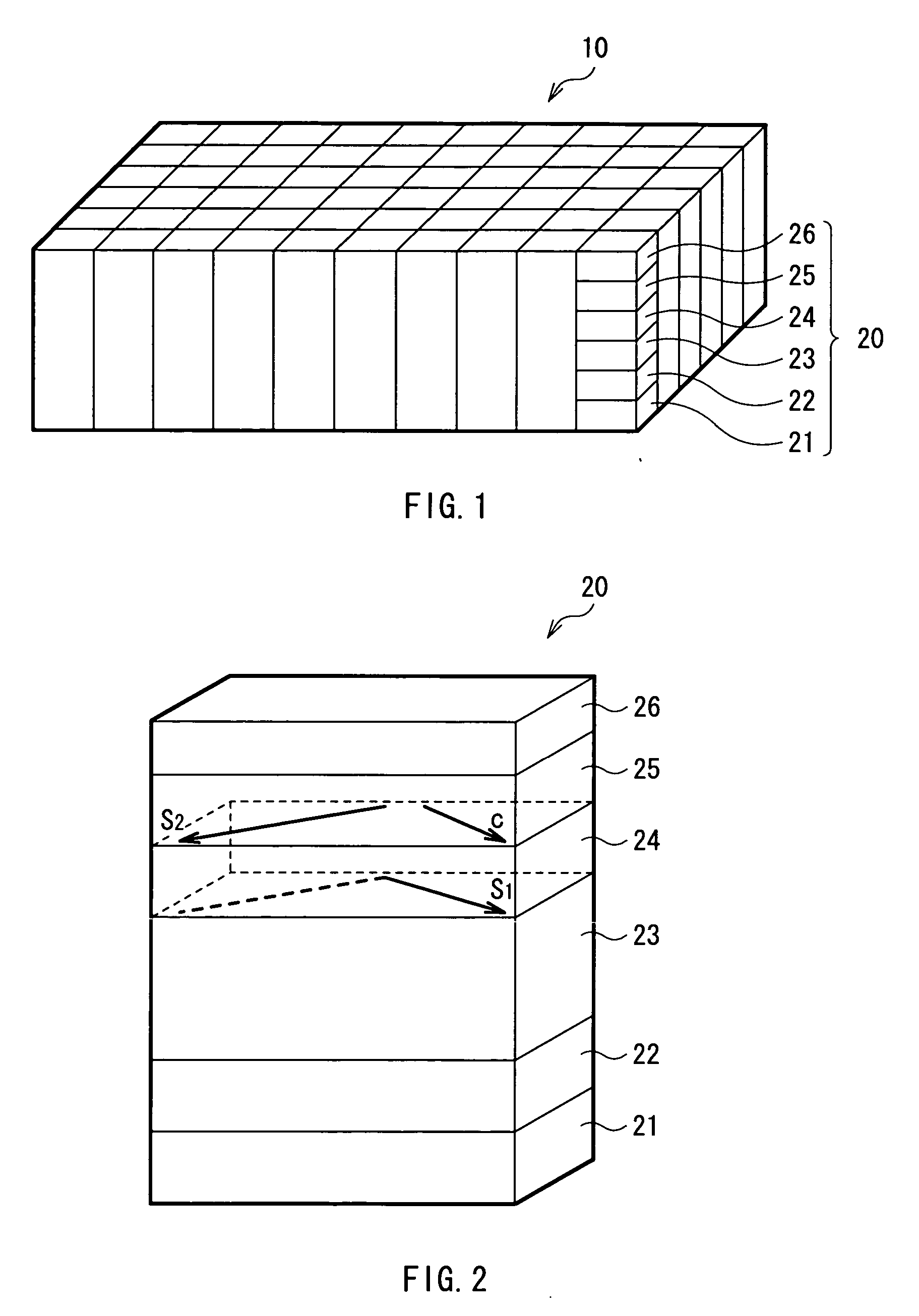
[0038]FIG. 1 shows a construction of a memory element according to a first embodiment of the invention. The memory element MM1 is a “spin injection type” element for performing writing by causing magnetization inversion by injecting polarized spin electrons. FIG. 2 shows a taken out memory cell 20 constructing the memory element MM1.

[0039] The memory element MM1 is a memory element wherein a plurality of memory cells 20 are arrayed in a state of a matrix (for example, array of M columns and N lines: M×N array). Recording information of the memory cell 20 is written by injecting a spin-polarized electron flow into each memory cell 20 (spin injection method). It is preferable that an in-plane size of this memory cell 20 is from 0.5 nm2 to 5 μm2. When the size of the memory cell is small, cross talk may be caused. It becomes possible to inhibit influence of a magnetic field due to a writing current to the adjacent respective memory cells 20 each other by setting to the foregoing size....

example

[0093] In this example, a nonvolatile RAM having the following construction was fabricated. Here, constructions from the electrode layer 26 to the substrate 21 will be shown.

[0094]

[0095] Electrode layer: Au film (25 nm thick)

[0096] Ferromagnetic free layer: permalloy film made of Ni81Fe19 (1 nm thick, and having uniaxial anisotropy so that the c axis becomes parallel to magnetization of the ferromagnetic fixed layer)

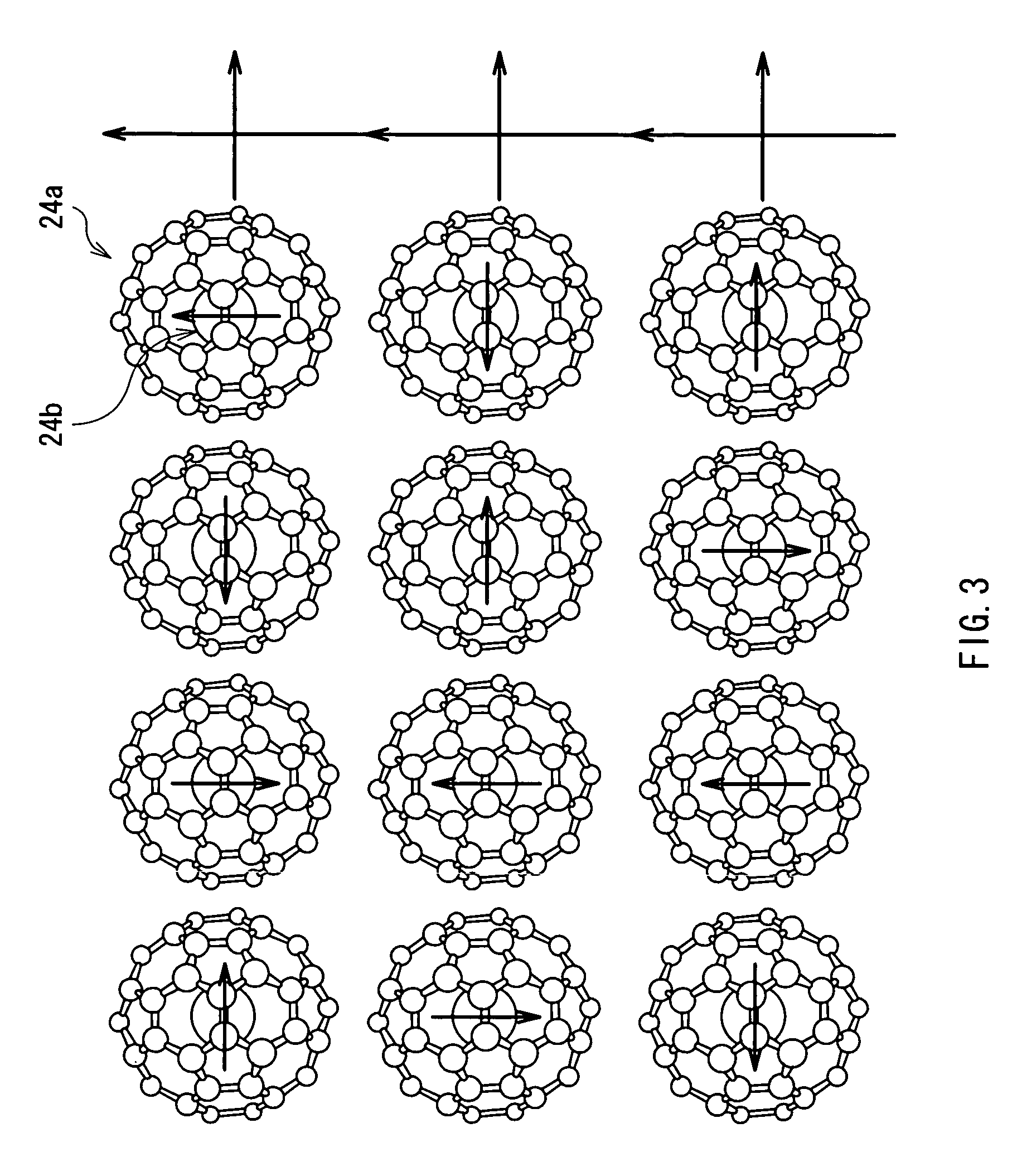
[0097] Paramagnetic layer: La@C82 thin film (20 nm thick)

[0098] Ferromagnetic fixed layer: permalloy film made of Ni81Fe19 (4 nm thick, and having uniaxial anisotropy)

[0099] Electrode layer: Au film (500 nm thick)

[0100] Substrate: silicon substrate

[0101] Measurement results of the sample structure of this example will be hereinafter shown.

[0102]

[0103] Polarization efficiency: to 90%

[0104] In-plane effective anisotropy magnetic field for ferromagnetic free layer: Hu=+2Ku / Ms to 10 Oe

[0105] Spin number density: to 1.9×1015 cm2

[0106] Gilbert attenuation coefficien...

second embodiment

[0147]FIG. 19 shows a construction of a memory element according to a second embodiment of the invention. This memory element MM2 is also “spin injection type” wherein writing is performed by generating magnetization inversion by injecting polarized spin electrons. A basic structure thereof is that a spin conduction layer 3 is provided between two ferromagnetic layers, that is, a fixed layer 1 wherein its magnetization orientation is fixed to a certain direction, and a free layer 2 wherein its magnetization orientation is changed by injecting the polarized spin electrons.

[0148] These respective layers are formed in layers inside a carbon nanotube 10 of one molecule. That is, the carbon nanotube 10 constructs one composition unit of a memory by setting a central part in the axis direction to the spin conduction layer 3, and including the fixed layer 1 and the free layer 2 in the both ends thereof Further, the fixed layer 1 and the free layer 2 are provided with electrode layers 4A a...


PUM


Abstract

A memory element wherein a spin conduction layer having a sufficient spin coherence length and a uniform spin field can be obtained, and thereby practical use is attained and a memory device are provided. A spin conduction layer (paramagnetic layer) (24) is a fullerene thin film being from 0.5 nm to 5 μm thick, for example. The fullerene has a hollow sized, for example, from 0.1 nm to 50 nm. A paramagnetic material is included in this hollow. A fermi vector of the fullerene thin film well laps over small number of spin band or plenty of spin band of a ferromagnetic fixed layer (23) and a ferromagnetic free layer (25). Further, spin orientations of the included paramagnetic material are random. Further, electron spin in the fullerene is in a quantized state in a pseudo zero dimensional space. Thereby, a spin coherence length becomes long in the fullerene thin film, and scatteration of spin-polarized conduction electrons goes away.

Description

TECHNICAL FIELD [0001] The present invention relates to a memory element for writing recording information by injecting spin-polarized electrons and a memory device using this memory element. BACKGROUND ART [0002] Under the circumstances that the high speed network society has come, in the mobile media rapidly becoming popular such as mobile phones and laptop computers, development of nonvolatile memories has been particularly required. The nonvolatile memory can retain data without being always supplied with electric power. Therefore, in the devices using the nonvolatile memory can be run immediately after the power is turned on. Further, power consumption can be reduced. [0003] A Magnetic Random Access Memory (MRAM) recently noted comprises high speed characteristics of a SRAM (Static RAM), high density and lower cost characteristics of a DRAM (Dynamic RAM), and nonvolatile characteristics of a flash memory. Therefore, the MRAM is considered as a promising memory of a future de fa...

Claims


Application Information

Patent Timeline
Patent Type & Authority Applications(United States)
IPC IPC(8): H01L37/00G11C11/16H01L27/105H01L27/22H01L43/08H01L43/10
CPCB82Y10/00B82Y30/00H01L43/08G11C13/025H01L27/222G11C11/16H10B61/00H10N50/10H01L27/105
Inventor KADONO, KOJIATA, MASAFUMI
Owner SONY CORP
Why Eureka
Try Eureka