Semiconductor device

a technology of semiconductor devices and semiconductors, applied in the direction of semiconductor devices, electrical equipment, transistors, etc., can solve the problems of difficult to provide high-degree integration of conventional semiconductor devices, and achieve the effect of increasing the degree of integration

Inactive Publication Date: 2006-01-12
RENESAS ELECTRONICS CORP
View PDF12 Cites 20 Cited by
  • Summary
  • Abstract
  • Description
  • Claims
  • Application Information

AI Technical Summary

Benefits of technology

[0008] The present invention contemplates a semiconductor dev

Problems solved by technology

As such, it has been difficult to provide conventional

Method used


Image

  • Semiconductor device
  • Semiconductor device
  • Semiconductor device

Examples


first embodiment

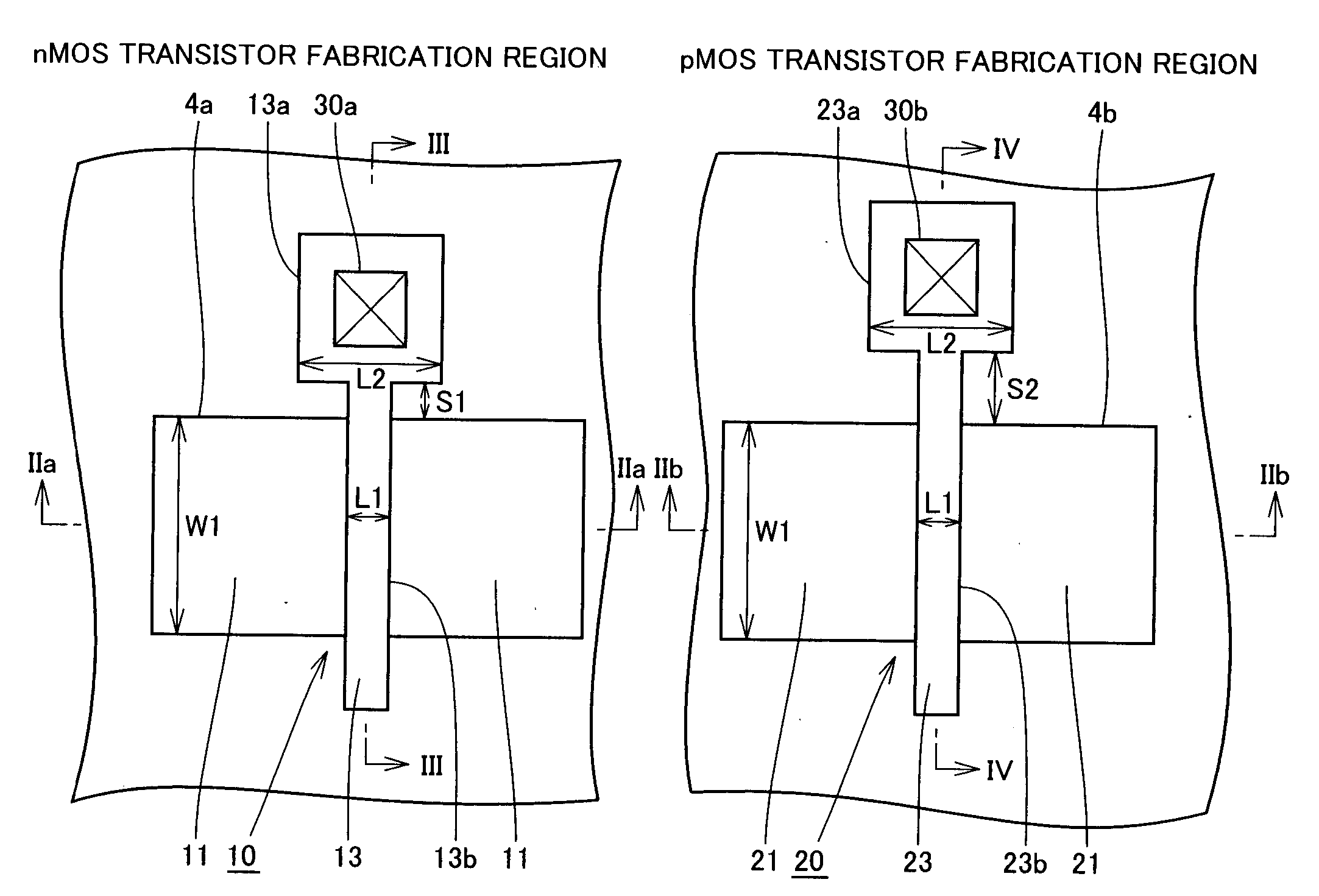
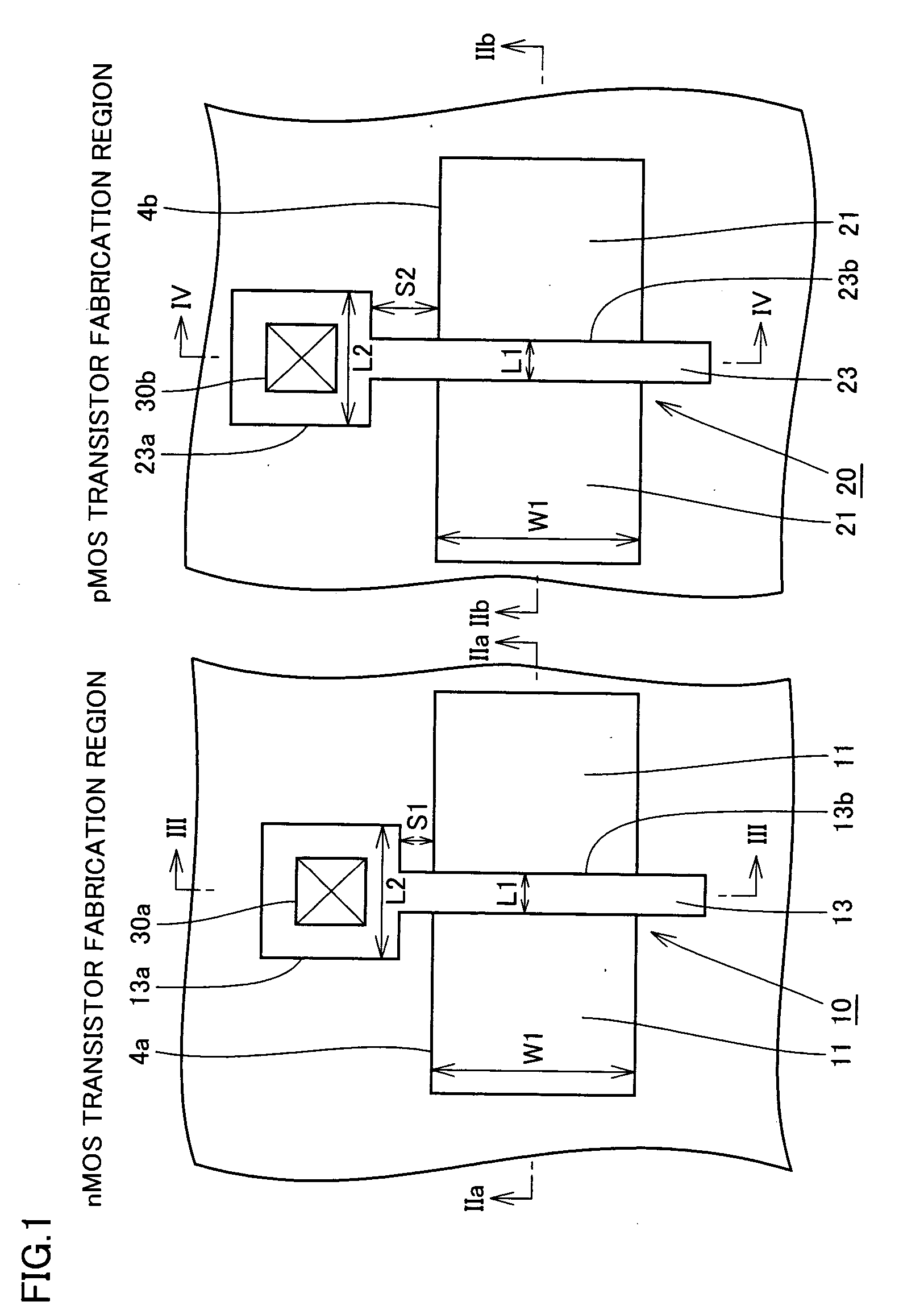
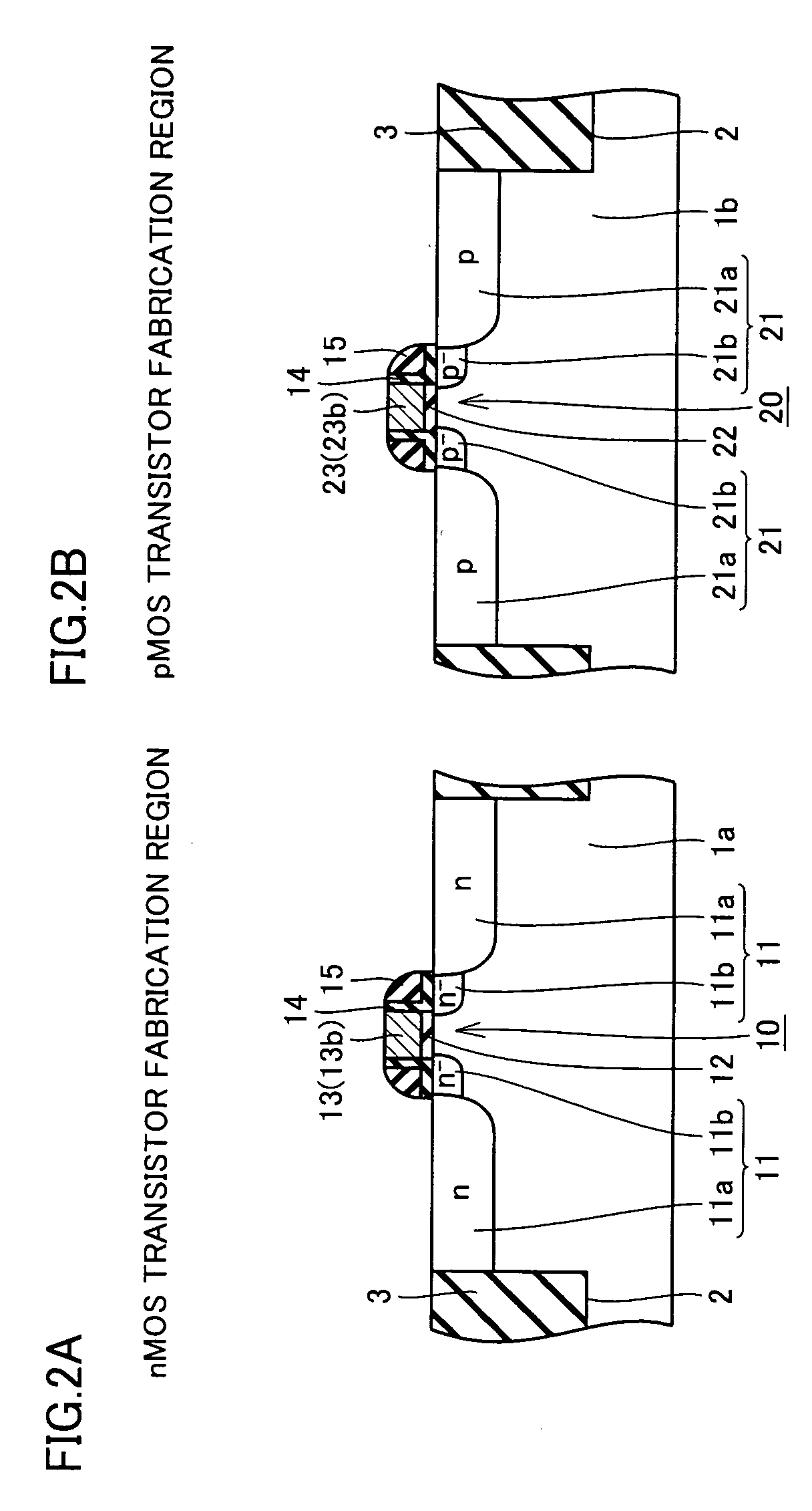
[0035]FIG. 1 is a plan view schematically showing a configuration of the present semiconductor device in a first embodiment. FIG. 2A is a schematic cross section taken along a line IIa-IIa of FIG. 1, and FIG. 2B is a schematic cross section taken along a line IIb-IIb of FIG. 1. FIG. 3 is a schematic cross section taken along a line III-III of FIG. 1. FIG. 4 is a schematic cross section taken along a line IV-IV of FIG. 1. Note that FIGS. 3 and 4 show a contact pad portion with a conductive layer connected thereto.

[0036] With reference to FIGS. 1 and 2A, in an nMOS transistor fabrication region a semiconductor substrate has a p well 1a having a surface selectively provided with an element isolation structure having a trench isolation structure for example including a trench 2 formed in a surface of the semiconductor substrate and an insulation layer 3 buried in trench 2. This element isolation structure surrounds an active region 4a, as seen in a plane, and thus electrically isolates...

second embodiment

[0067]FIG. 11 is a plan view schematically showing a configuration of the present semiconductor device in a second embodiment and FIG. 12 is a schematic cross section taken along a line XII-XII line of FIG. 11. With reference to the figures, in the present embodiment, gate electrode 113 has a uniform width along its entire length. Gate electrode layer 113 is covered with interlayer insulation layer 31 provided with a hole 31c reaching gate electrode layer 113.

[0068] In hole 31c is provided a conductive layer 32c for electrically connecting an overlying line to gate electrode layer 113. Conductive layer 32c is connected to gate electrode layer 113 by contact 130. A portion shown in FIG. 11 that is taken along a line IIa-IIa provides a cross section similar in configuration to that shown in FIG. 2A.

[0069] Other than the above described feature, the present embodiment provides a configuration substantially similar to that of the first embodiment. Accordingly, identical components are...


PUM


Abstract

In an active region a pair of source/drain regions of an nMOS transistor is provided. Between the paired source/drain regions the semiconductor substrate has a region provided with a gate electrode layer with a gate oxide film interposed. The gate electrode layer extends on both the active region and an element isolation structure and also has a contact pad portion on the element isolation structure, and the active region and the contact pad as seen in a plane are spaced by less than 0.5 μm.

Description

BACKGROUND OF THE INVENTION [0001] 1. Field of the Invention [0002] The present invention relates generally to semiconductor devices and particularly to semiconductor devices having a metal insulator semiconductor (MIS) transistor. [0003] 2. Description of the Background Art [0004] When a minimally dimensioned complementary metal oxide semiconductor (CMOS) circuit is configured, its device is designed in accordance with a design rule defined for each generation. For example, for a transistor, a gate's pitch space, an active region's area and the like are determined in accordance with the design rule. Generally, this design rule is common between n channel MOS (nMOS) and p channel MOS (pMOS) transistors. [0005] Such a transistor has a gate electrode laid out as shown for example in Japanese Patent Laying-Open No. 09-129744. [0006] Conventionally a gate electrode has a contact pad portion having a structure larger in width than a gate portion to prevent a contact from stepping out a s...

Claims


Application Information

Patent Timeline
IPC IPC(8): H01L29/76
CPCH01L21/76895H01L27/092H01L27/0207
Inventor TSUBOI, NOBUO
Owner RENESAS ELECTRONICS CORP
Why Eureka
Try Eureka