Semiconductor device and semiconductor module employing thereof

a semiconductor module and semiconductor technology, applied in semiconductor devices, semiconductor/solid-state device details, electrical apparatus, etc., can solve the problems of increasing the filling time, reducing the density of the through electrode, and reducing the filling time, so as to achieve a small area and a higher density

Active Publication Date: 2006-01-12
TESSERA ADVANCED TECH
View PDF3 Cites 69 Cited by
  • Summary
  • Abstract
  • Description
  • Claims
  • Application Information

AI Technical Summary

Benefits of technology

[0027] According to the present invention, there is provided a semiconductor module, comprising a multilayered structure that includes the semiconductor device according to the present invention and other type of semiconductor device, wherein the first electric conductor or the second electric conductors is electrically coupled to the othe

Problems solved by technology

However, it has now been discovered that, since one through plug corresponds to one interconnect in the techniques described in the above-described related art, it has been difficult to improve the density of the through electrodes.
In addition, these techniques have left rooms for improvement, in view of the difficulty in reducing the parasitic capacitance and further the difficulty in providing additional functions to the through plug.
While the thickness of the insulating film should be thicker in order to reduce the capacity, the increased thickness causes an increase of the filling time.
When a ring-shaped structure having no sl

Method used


Image

  • Semiconductor device and semiconductor module employing thereof
  • Semiconductor device and semiconductor module employing thereof
  • Semiconductor device and semiconductor module employing thereof

Examples


first embodiment

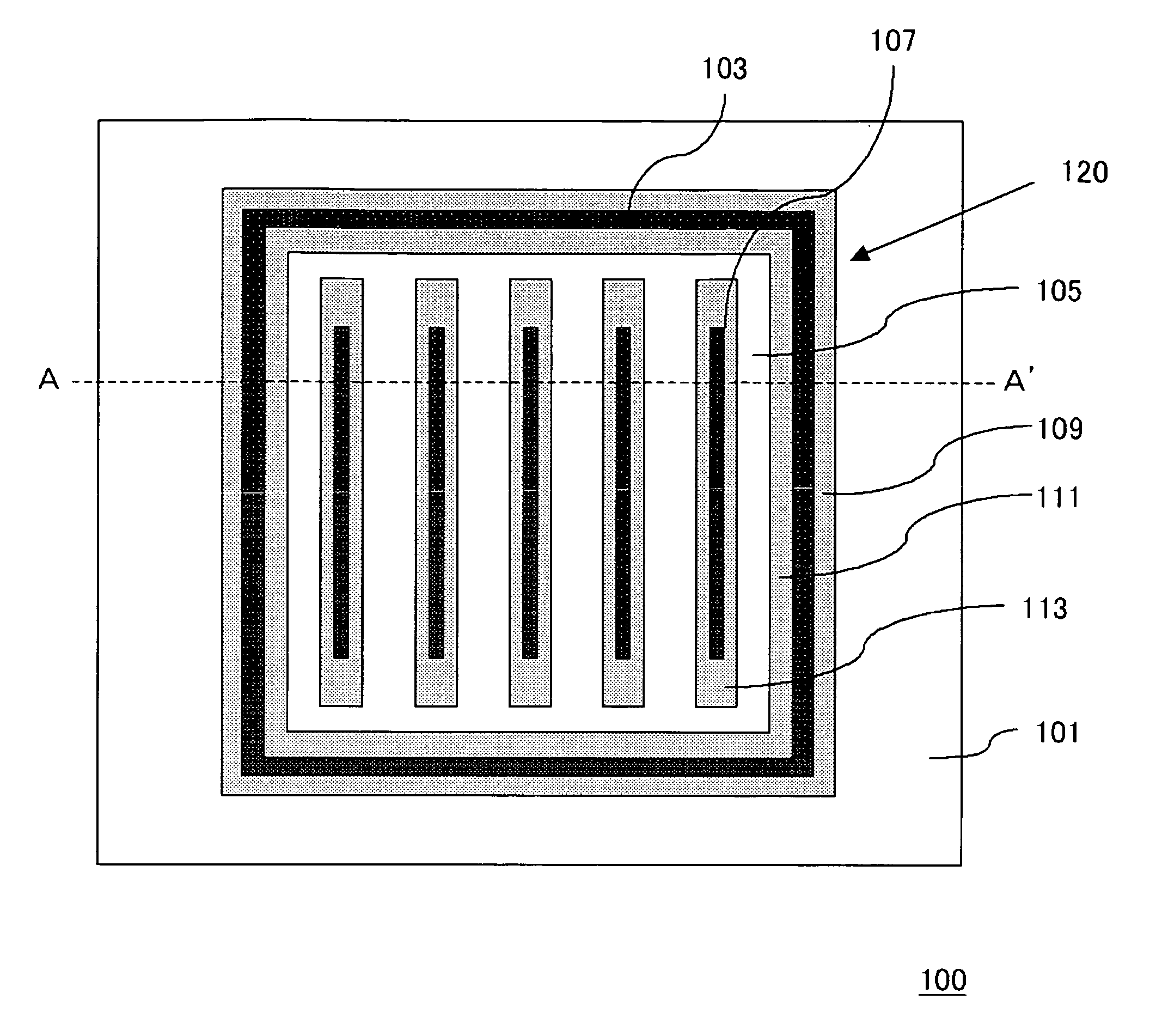
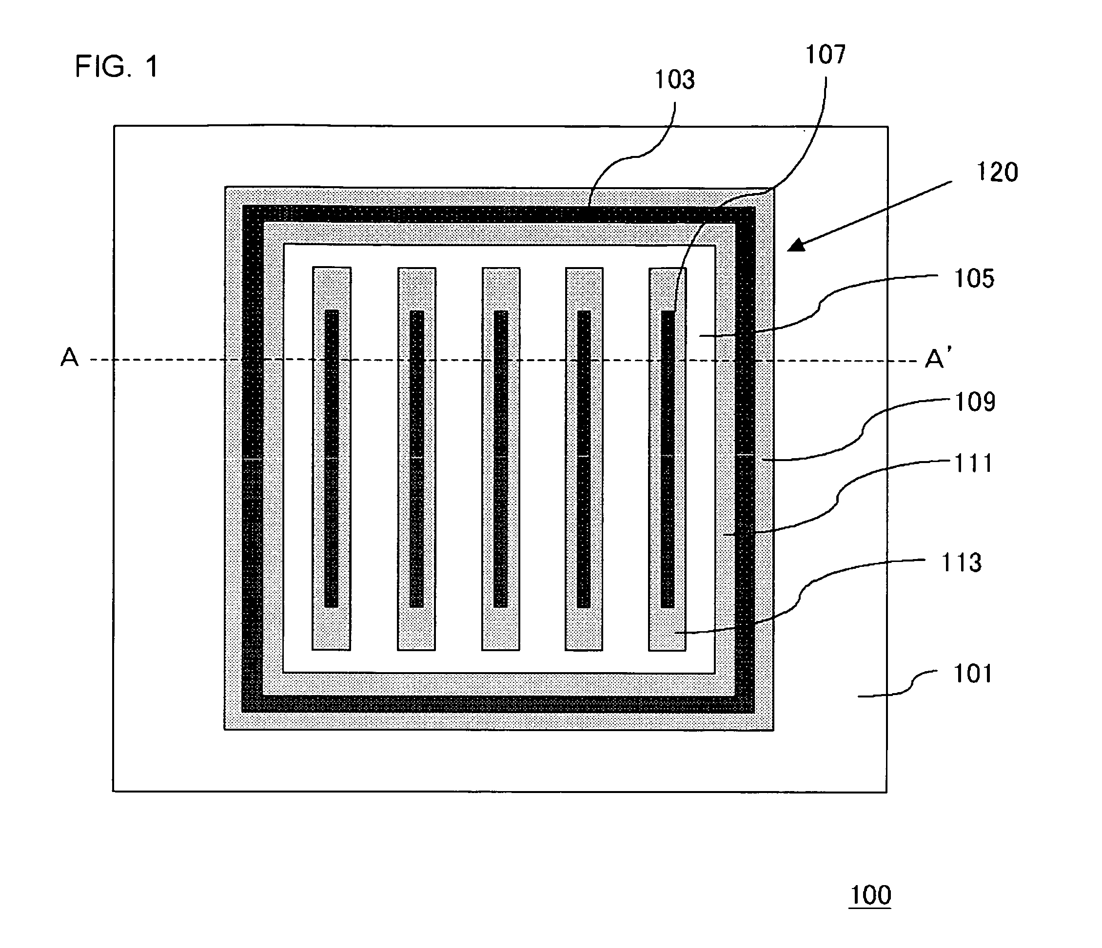
[0045] The present embodiment relates to a semiconductor device that comprises a through electrode. One or more stripe-shaped through electrode(s) are disposed in a mutually vicinity on the semiconductor substrate, and a pipe-shaped through electrode having a predetermined width encloses the outside of the stripe-shaped through electrodes.

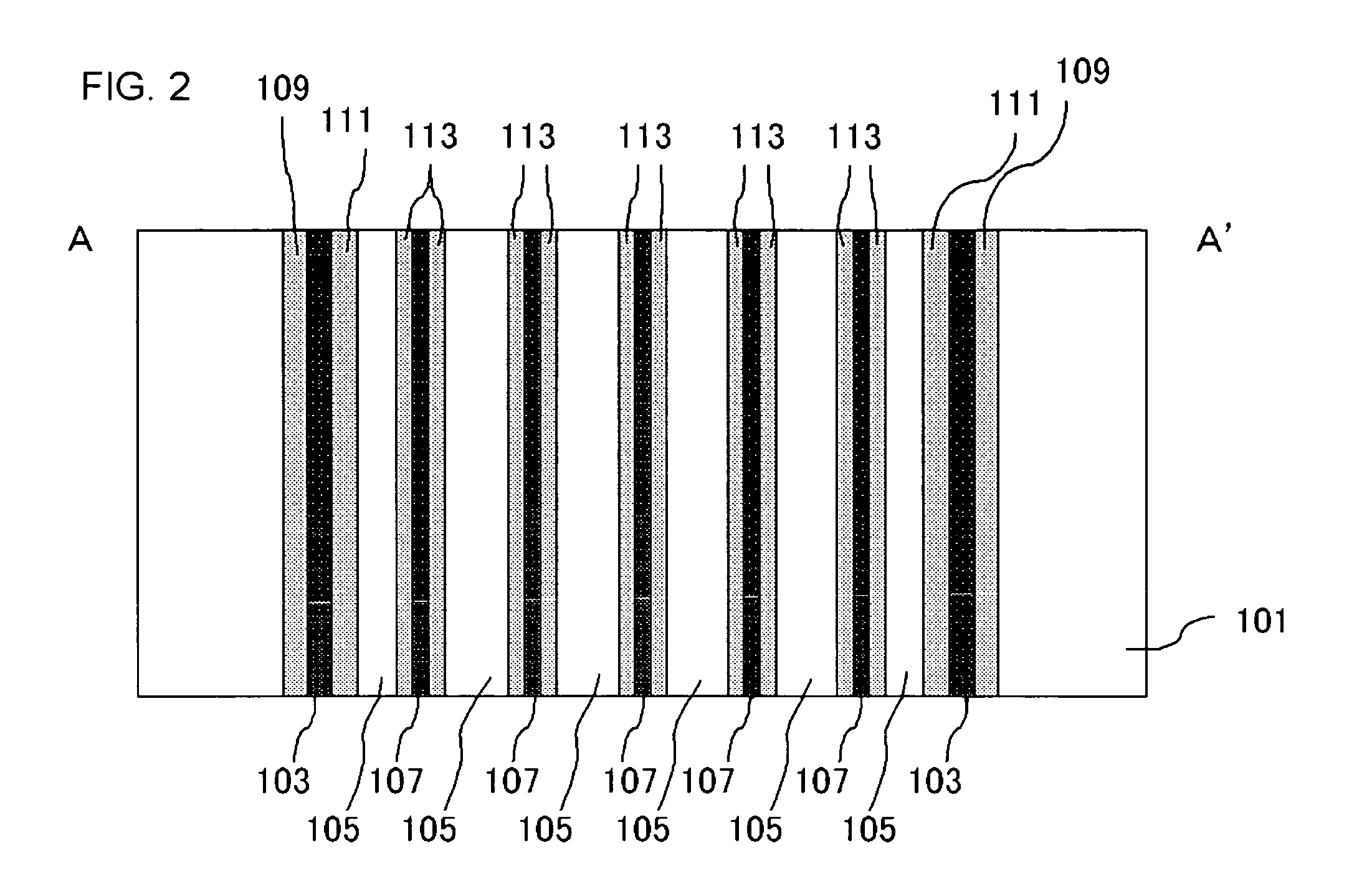
[0046]FIG. 1 is a view, schematically showing a configuration of a semiconductor device according to the present embodiment. FIG. 2 is a cross-sectional view of FIG. 1 along A-A′. The semiconductor device 100 shown in FIG. 1 includes a silicon substrate 101 and a structure 120 filled within through holes having rectangular cross-sections that extends through (penetrates) the silicon substrate 101. The structure 120 comprises a pipe-shaped through electrode 103, stripe-shaped through electrodes 107, silicons 105, a first insulating film 109, a second insulating film 111 and third insulating films 113.

[0047] The pipe-shaped through electrode 103 is...

second embodiment

[0080]FIG. 3 is a cross-sectional view, schematically showing a configuration of a semiconductor device according to the present embodiment. FIG. 4 is a B-B′ cross-sectional view of FIG. 3. As shown in FIG. 3 and FIG. 4, a semiconductor device 110 comprises a silicon substrate 101 and a structure 130 extending through (penetrating) the silicon substrate 101. The structure 130 comprises through electrodes 131, silicons 119, a first insulating film 109 and a second insulating film 133.

[0081] The through electrode 131 is a continuous and integrated member of a pipe-shaped through electrode 115 and a stripe-shaped through electrodes 117. The pipe-shaped through electrode 115 is a pipe-shaped electric conductor extending through (penetrating) the silicon substrate 101. Two-dimensional shape of the pipe-shaped through electrode 115 is a rectangular loop.

[0082] Further, the stripe-shaped through electrodes 117 extend through (penetrate) the silicon substrate 101 to couple a region of the...

third embodiment

[0094] The semiconductor devices described in the above embodiments can preferably be employed in the multi-chip modules. The multi-chip module may have a configuration, in which, for example, the semiconductor devices according to the above embodiments and other type of semiconductor devices are stacked, and the through electrode extending through (penetrating) the silicon substrate 101 and the conductive member of other semiconductor device are electrically coupled.

[0095]FIG. 9 is a cross-sectional view, schematically showing a configuration of a multi-chip module having a configuration that plurality of (three for the case of FIG. 9) layers of the semiconductor device 110 described in the second embodiment (FIG. 3) are stacked. In FIG. 9, the through electrodes 131 provided in each of the semiconductor devices 110 are linearly arranged toward a direction that is perpendicular to the face of the silicon substrate 101. Adjacent through electrodes 131 are coupled with each other th...


PUM


Abstract

A semiconductor device 100 is provided with a silicon substrate 101 and a structure 120 filled in a through hole that has a rectangular cross section and extends through the silicon substrate 101. The structure 120 comprises a pipe-shaped through electrode 103, stripe-shaped through electrodes 107, silicons 105, a first insulating film 109, a second insulating film 111 and a third insulating film 113. The pipe-shaped through electrode 103 is utilized as a pipe-shaped electric conductor that extends through the silicon substrate 101. In addition, the stripe-shaped through electrodes 107 are provided in the interior of the pipe-shaped through electrode 103 so that the stripe-shaped through electrodes 107 extend through the silicon substrate 101 and is spaced away from the pipe-shaped through electrode 103. A plurality of through electrodes 107 are provided in substantially parallel within the inner region of the pipe-shaped through electrode 103.

Description

[0001] This application is based on Japanese patent application NO. 2004-194673, the content of which is incorporated hereinto by reference. BACKGROUND OF THE INVENTION [0002] 1. Field of the Invention [0003] The present invention relates to a semiconductor device comprising through electrodes and a semiconductor module employing thereof. [0004] 2. Related Art [0005] In the conventional technique, bare chip stacked-type multi-chip module (MCM) has been proposed for the purpose of achieving higher degree of integration over a SiP of a package stacked-type or a type of having arranged chips in parallel. An interconnect extending through the semiconductor substrate is essential for the bare chip stacked-type module. Exemplary conventional bare chip stacked-type MCMs having a through electrode are described in Japanese Patent Laid-Open No. 1998-223,833 (H10-223,833), Japanese Patent Laid-Open No. 2002-170,904, Japanese Patent Laid-Open No. 2002-289,623 and Japanese Patent Laid-Open No. ...

Claims


Application Information

Patent Timeline
IPC IPC(8): H01L23/48
CPCH01L23/481H01L23/585H01L2224/16H01L2225/06513H01L25/0657H01L24/05H01L2224/0401H01L2224/05009H01L2224/05551H01L2224/05552H01L2224/05553H01L2224/05555H01L2224/13025H01L2224/14181H01L2224/16146H01L2224/16225
Inventor MATSUI, SATOSHIKAWANO, MASAYA
Owner TESSERA ADVANCED TECH
Why Eureka
Try Eureka