Eureka AIR delivers breakthrough ideas for toughest innovation challenges, trusted by R&D personnel around the world.

On-chip amplifier/line driver compensation circuit

Inactive Publication Date: 2006-01-12
AVAGO TECH INT SALES PTE LTD
View PDF12 Cites 1 Cited by
  • Summary
  • Abstract
  • Description
  • Claims
  • Application Information

AI Technical Summary

Benefits of technology

[0012] The present invention is directed to an on-chip amplifier/line driver compensation circu

Problems solved by technology

Also, it is generally not desirable to restrict a particular application to using a specific package.
Thus, stability becomes a problem for such high bandwidth amplifiers due to the introduction of additional phase (especially for low closed loop operation).
The package parasitics also become a bigger problem at higher frequencies.
This causes significant phase shift at high frequencies and results in instability, which can manifest itself as oscillation, or ringing, resulting in poor or unacceptable performance.
However, this requires an extra terminal to be brought out to the package 201, which is not desirable, and which can also add board noise back into the chip.

Method used


Image

  • On-chip amplifier/line driver compensation circuit
  • On-chip amplifier/line driver compensation circuit
  • On-chip amplifier/line driver compensation circuit

Examples


Embodiment Construction

[0021] Reference will now be made in detail to the embodiments of the present invention, examples of which are illustrated in the accompanying drawings.

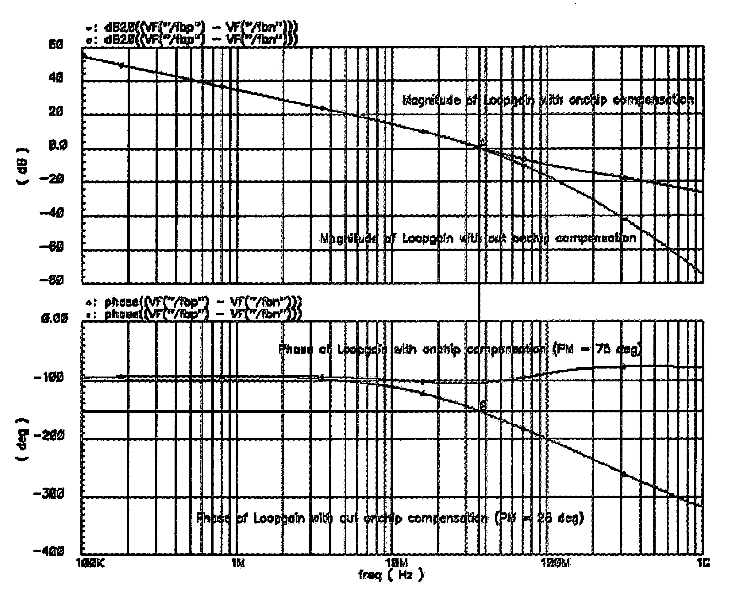
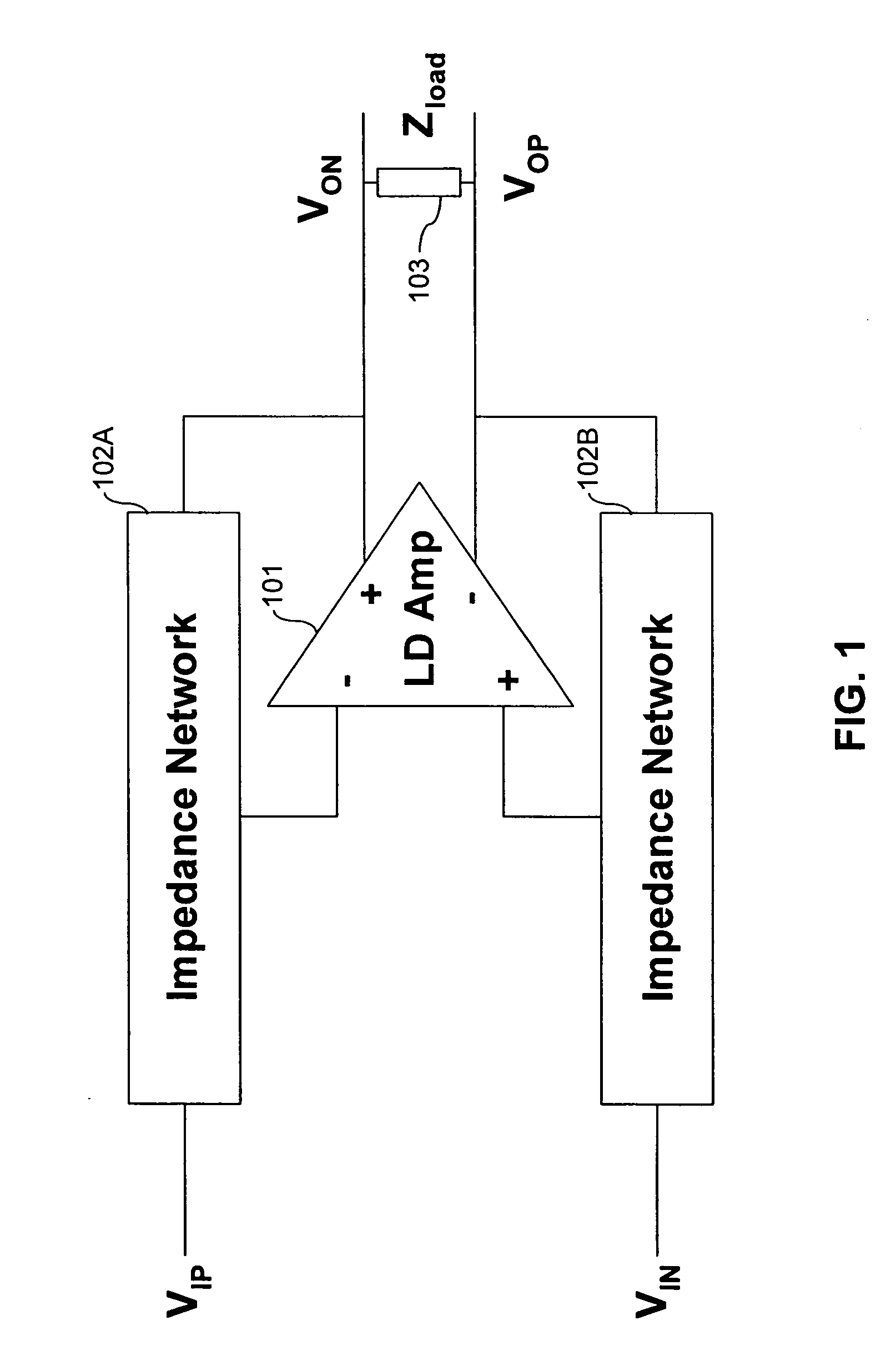
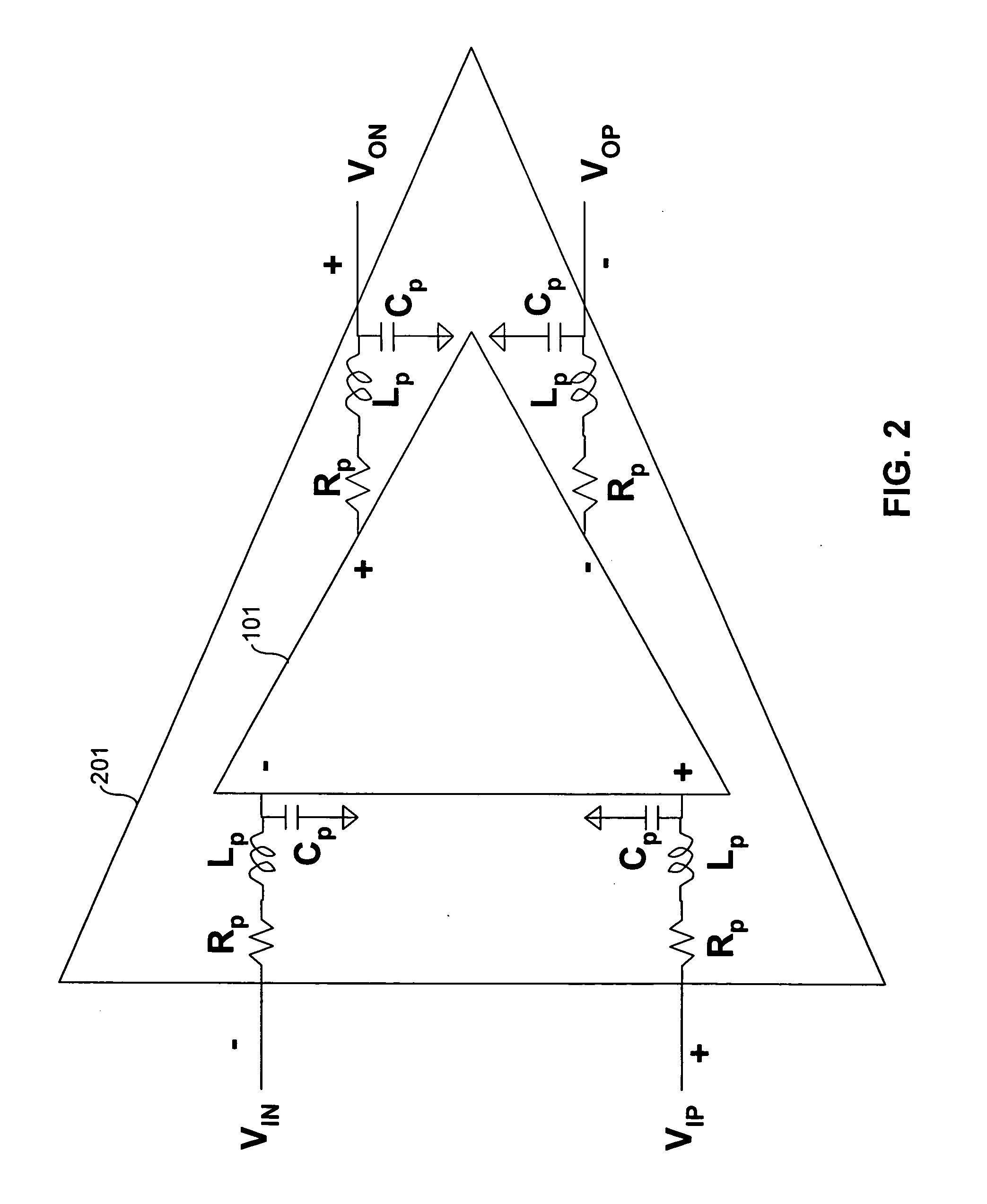
[0022]FIG. 3 illustrates one embodiment of the present invention. As shown in FIG. 3, an amplifier 101 is packaged within a package 201. Outputs VON, VOP are shown with the lumped parasitics RP, LP and CP. Inputs VIN, VIP are also shown with the lumped parasitics RP, LP, CP. Cg is the input capacitance of the amplifier 101, which is a known value for a given amplifier 101. In order to provide the appropriate phase response at the desired frequency of operation, feedback capacitances Ccf1 and Ccf2 have been added to the amplifier chip. These added feedback capacitors serve to keep a feedback factor of the amplifier 101 appropriate for high frequency operation. Thus, the amplifier 101 is stable in a closed loop configuration even when the values of the parasitic impedances are high. Note that one of the advantages of the approach desc...


PUM


Abstract

An embodiment of the present invention includes an amplifier on an integrated circuit, with the amplifier having positive and negative inputs, and positive and negative outputs. A first feedback capacitor is on the integrated circuit between the positive input and the negative output. A second feedback capacitor is on the integrated circuit between the negative input and the positive output. A package encloses the integrated circuit. A third capacitor is between the positive and negative inputs. A feedback factor of the amplifier circuit approaches unity. In example embodiments, the first and second capacitors are between 3 and 10 pF. The third capacitor is between 3 and 10 pF.

Description

BACKGROUND OF THE INVENTION [0001] 1. Field of the Invention [0002] The present invention relates to differential line drivers, and more particularly, to low distortion high speed differential drivers. [0003] 2. Related Art [0004] Transmit line driver amplifiers typically need to drive a very low ohmic loads and need to be stable and operate with a high linearity in a variety of feedback configurations. These can include pure resistive gain configurations, or configurations with gain and some filtering embedded in the feedback network (see FIG. 1). As shown in FIG. 1, a line driver amplifier configuration includes an amplifier 101 having differential outputs VOP, VON driving a load 103. Differential inputs to the amplifier 101 include VIP and VIN, optionally passing through an impedance feedback network 102A, 102B. Note that in FIG. 1, the power supply and ground connections are not shown, since they are outside of the signal path. [0005] To maintain high linearity, the open-loop am...

Claims


Application Information

Patent Timeline
IPC IPC(8): H03F3/45
CPCH03F1/08
Inventor RANGANATHAN, SUMANT
Owner AVAGO TECH INT SALES PTE LTD
Why Eureka
Eureka Blog
Learn More