Display device and driving method thereof

Inactive Publication Date: 2006-01-12
SAMSUNG ELECTRONICS CO LTD
View PDF7 Cites 236 Cited by
  • Summary
  • Abstract
  • Description
  • Claims
  • Application Information

AI Technical Summary

Benefits of technology

[0017] A method embodiment of driving a display device including first pixels is also provided, each of the first pixels including a first light emitting element and a first driving transistor supplying current to the first light emitting element, the method including sequentially writing first data signals to the first pixels; simultaneously emitting the first light emitting elements based on the written data signals after the writing of the first data signals for all the first pixels is finished; and simultaneously supplying a reverse bias to the first driving transistors, wherein the emission of the first light emitting elements is suppressed during the writing of the first data signals.
[0018] The suppression of the light emission of the first light emitting elements may include decreasing a magnitude of a voltage applied to the first light emitting elements through the first driving transistors. The display device may further include second pixels, each of the second pixel including a second light emitting element and a second driving transistor supplying current to the second light emitting element, and the method may further include sequen

Problems solved by technology

A polysilicon TFT has several advantages, but it also has disadvantages such as the complexity of manufacturing polysilicon, thereby increasing the manufacturing cost.
In addition, it is hard to make a large O

Method used


Image

  • Display device and driving method thereof
  • Display device and driving method thereof
  • Display device and driving method thereof

Examples


Embodiment Construction

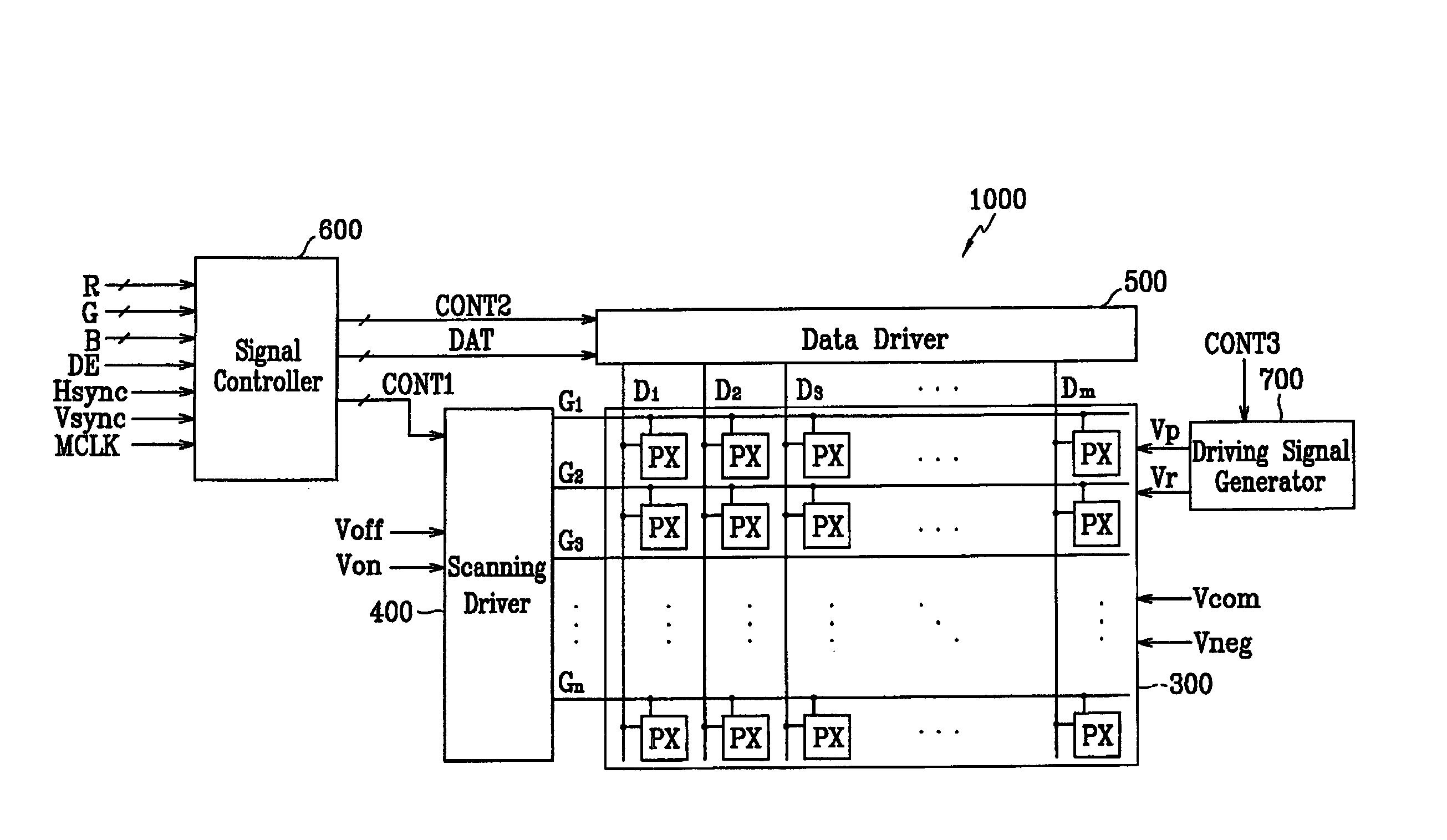
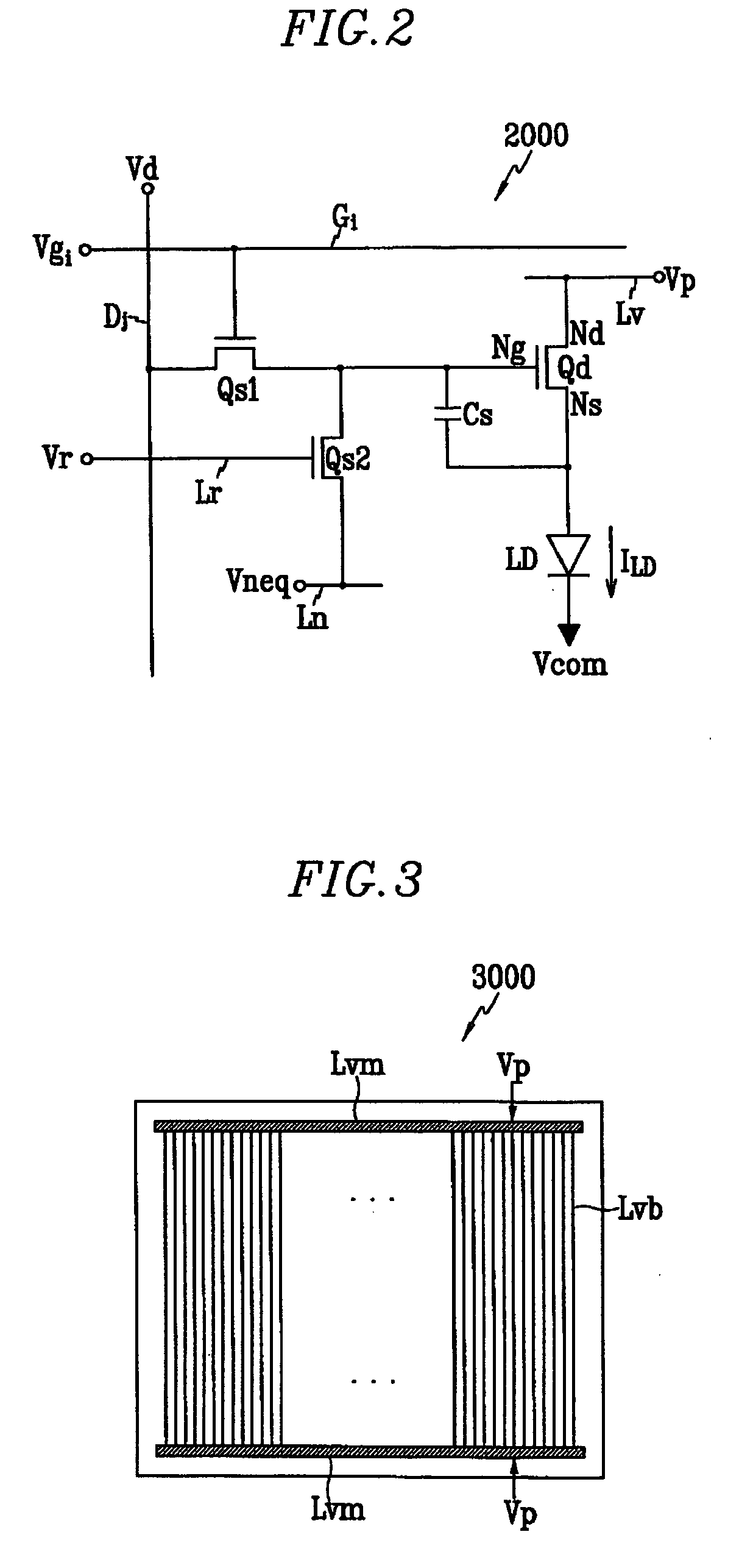
[0034] The present invention now will be described more fully hereinafter with reference to the accompanying drawings, in which preferred embodiments of the disclosure are shown. In the drawings, the thickness of layers and regions may be exaggerated for clarity. Like reference numerals may refer to like elements throughout the drawings. It will be understood that when an element such as a layer, region or substrate is referred to as being “on” another element, it can be directly on the other element or intervening elements may also be present. In contrast, when an element is referred to as being “directly on” another element, there are no intervening elements present. Exemplary display devices and driving methods thereof according to embodiments of the present disclosure will be described with reference to the accompanying drawings.

[0035] Referring to FIGS. 1-7, an organic light emitting display (OLED) according to an embodiment of the present disclosure will be described in detai...


PUM


Abstract

A display device is provided, including light emitting elements, first switching transistors transmitting data signals in response to scanning signals, second switching transistors transmitting a reverse bias voltage in response to a switching signal, capacitors charging voltages based on the data signals and discharging based on the reverse bias voltage; and driving transistors, each driving a transistor connected to a driving voltage and turning on and off in response to the voltage charged in the capacitor to connect and disconnect a signal passage from the driving voltage to the light emitting element.

Description

BACKGROUND OF THE INVENTION [0001] (a) Field of the Invention [0002] The present disclosure relates to display devices and driving methods, and more particularly relates to a light emitting display device and a driving method thereof. [0003] (b) Description of Related Art [0004] Recent trends in lighter-weight and thinner personal computers and televisions sets call for correspondingly lighter-weight and thinner display devices. In addition, flat panel displays satisfying such requirements are being substituted for conventional cathode ray tubes (CRT). The flat panel displays may include a liquid crystal display (LCD), field emission display (FED), organic light emitting display (OLED), plasma display panel (PDP), or the like. [0005] Generally, an active matrix flat panel display includes a plurality of pixels arranged in a matrix and displays images by controlling the luminance of the pixels based on given luminance information. An OLED is a self-emissive display device that displa...

Claims


Application Information

Patent Timeline
IPC IPC(8): G09G3/30H01L51/50G09G3/20H05B33/14
CPCG09G3/3233G09G3/3291G09G2300/0426G09G2300/0842G09G2300/0866G09G2310/0254G09G2310/0251G09G2310/0256G09G2310/08G09G2320/043G09G2310/0218G09G3/30
Inventor CHOI, BEOHM-ROCKHUH, JONG-MOOCHOI, JOON-HOOKO, CHUN-SEOKPARK, CHEOL-WOOKIM, NAM-DEOG
Owner SAMSUNG ELECTRONICS CO LTD
Why Eureka
Try Eureka