Liquid crystal display device and electronic apparatus
Inactive Publication Date: 2006-01-12
SEIKO EPSON CORP
View PDF29 Cites 21 Cited by
Summary
Abstract
Description
Claims
Application Information
AI Technical Summary
This helps you quickly interpret patents by identifying the three key elements:
Problems solved by technology
Method used
Benefits of technology
Benefits of technology
[0012] An advantage of the invention is that it provides a highly reliable liquid crystal display device which provides a higher display quality and a high definition.
[0013] A liquid crystal display device according to a first aspect of the invention comprises a pair of opposing substrates and a liquid crystal layer disposed between the pair of substrates, the liquid crystal layer being formed of liquid crystal which has a negative dielectricanisotropy and which is vertically aligned in an initial alignment state. At least one columnar spacer is disposed at at least one of the substrates for separating the opposing substrates. Pixel areas are disposed in a matrix at either one of the pair of substrates in a plane thereof, each pixel area including a pixel electrode, a gap between the pixel electrode and an adjacent pixel electrode, a switching element connected to the pixel electrode, and a metallic line connected to the switching element. The spacer is disposed in at least one of the gaps or so as to overlap at least one of the switching elements in at least one of the pixel areas. At least one first protrusion having a height that is less than the height of the spacer is disposed in at least one of the pixel areas where the spacer is not provided. The location where the spacer is disposed and the location where the first protrusion is disposed in the respective pixel areas are in correspondence with each other.
[0014] According to the first aspect of the invention, the term “pixel area” does not refer to an area including only a pixel electrode. It refers to an area also including a signal line and an active element associated with one pixel electrode and a portion between the pixel electrode and an adjacent pixel electrode.
[0015] In this structure, since the number of columnar spacers can be reduced to the minimum required by disposing at least one columnar spacer only at at least one of the predetermined pixel areas in the display surface of the liquid crystal display device, it is possible to prevent bubbles from being produced in the liquid crystal layer particularly, at a low temperature. Hitherto, a difference had occurred between the liquid crystal alignment state of a pixel area where a columnar spacer is not disposed and that of a pixel area where a columnar spacer is disposed due to the influence of the columnar spacer, thereby reducing the display quality.
[0016] According to the structure, in the pixel area or areas where a columnar spacer or columnar spacers are not disposed, instead of the columnar spacer or columnar spacers, a protrusion or protrusions formed of, for example, resin is / are disposed substantially at a location or locations in correspondence with where the columnar spacer or columnar spacers are disposed in order to control the liquid crystal alignment. By making similar the influence of the columnar spacer or columnar spacers on the liquid crystal alignment and the influence of the first protrusion or first protrusions on the liquid crystal alignment, it is possible to reduce the difference between the liquid crystal alignment states at the pixel areas regardless of whether or not a columnar spacer is provided. Therefore, a high quality, highly reliable liquid crystal display device can be provided.
[0017] It is preferable that an area of an area where the spacer is disposed and an area of an area where the first protrusion is disposed be substantially the same.
Therefore, the liquid crystal is brought out of alignment, causing the display to appear uneven.
Since bubbles tend to be formed in a liquid crystal panel as the number of columnar spaces per unit area increases, the columnar spaces cannot be disposed in all pixel areas in a plane, particularly, in a high-definition liquid crystal display device.
This deteriorates display quality.
Hitherto, a difference had occurred between the liquid crystal alignment state of a pixel area where a columnar spacer is not disposed and that of a pixel area where a columnar spacer is disposed due to the influence of the columnar spacer, thereby reducing the display quality.
In a structure in which switching elements are provided, distortion of an electrical field generated from the switching elements destroys the symmetry of the electrical field in the liquid crystal layer and is thus a major cause of disturbing the liquid crystal alignment.
A relatively high voltage applied to the metallic lines causes the electrical field generated from the metallic lines to symmetrically distort the electrical field in the liquid crystal layer and thus to disturb the liquid crystal alignment.
Therefore, the switching elements tend to be damaged by external pressure, such as push pressure.
Method used
Image
Click on the blue label to locate the original text in one second.
Reading with bidirectional positioning of images and text.
Examples
first embodiment
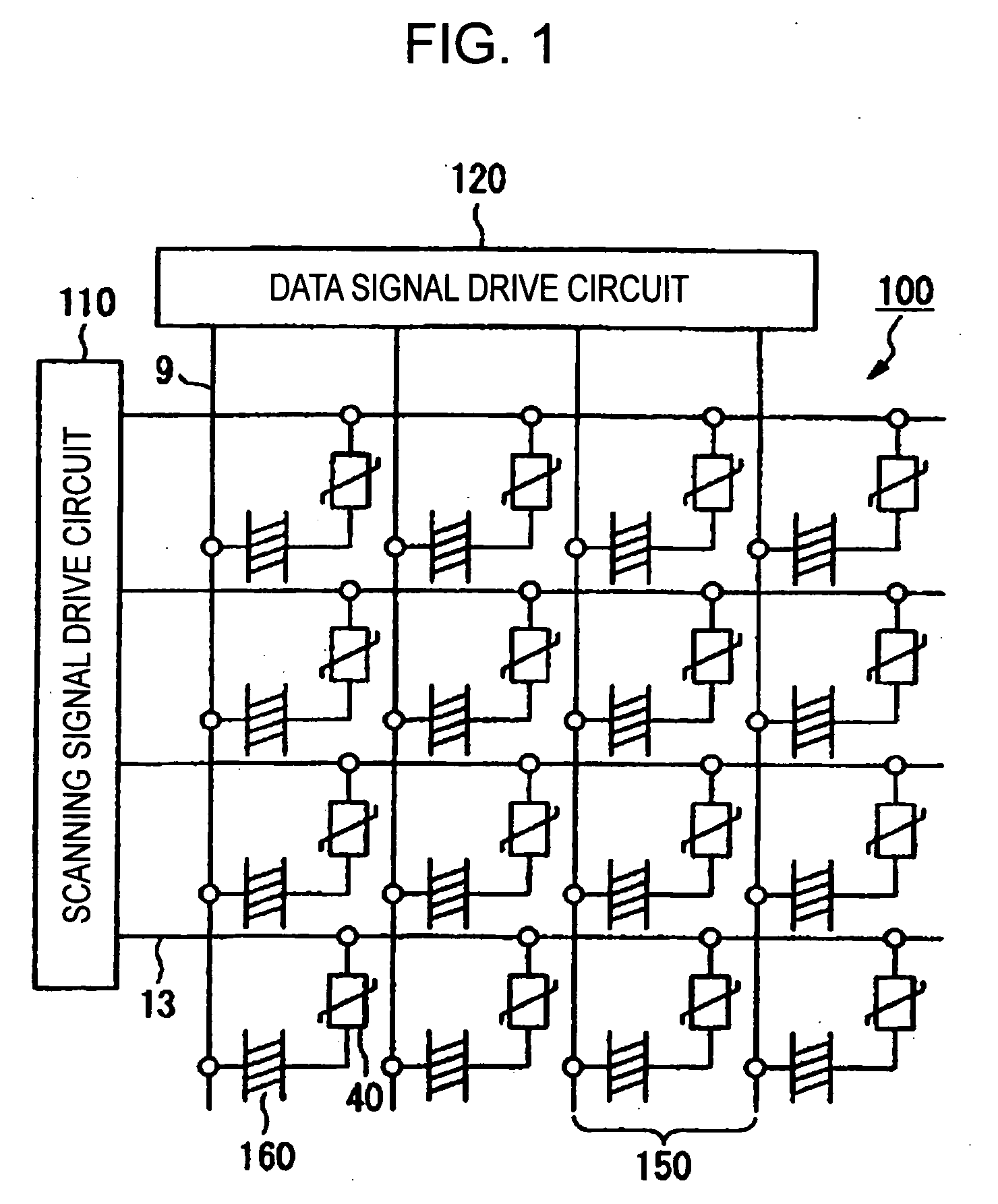
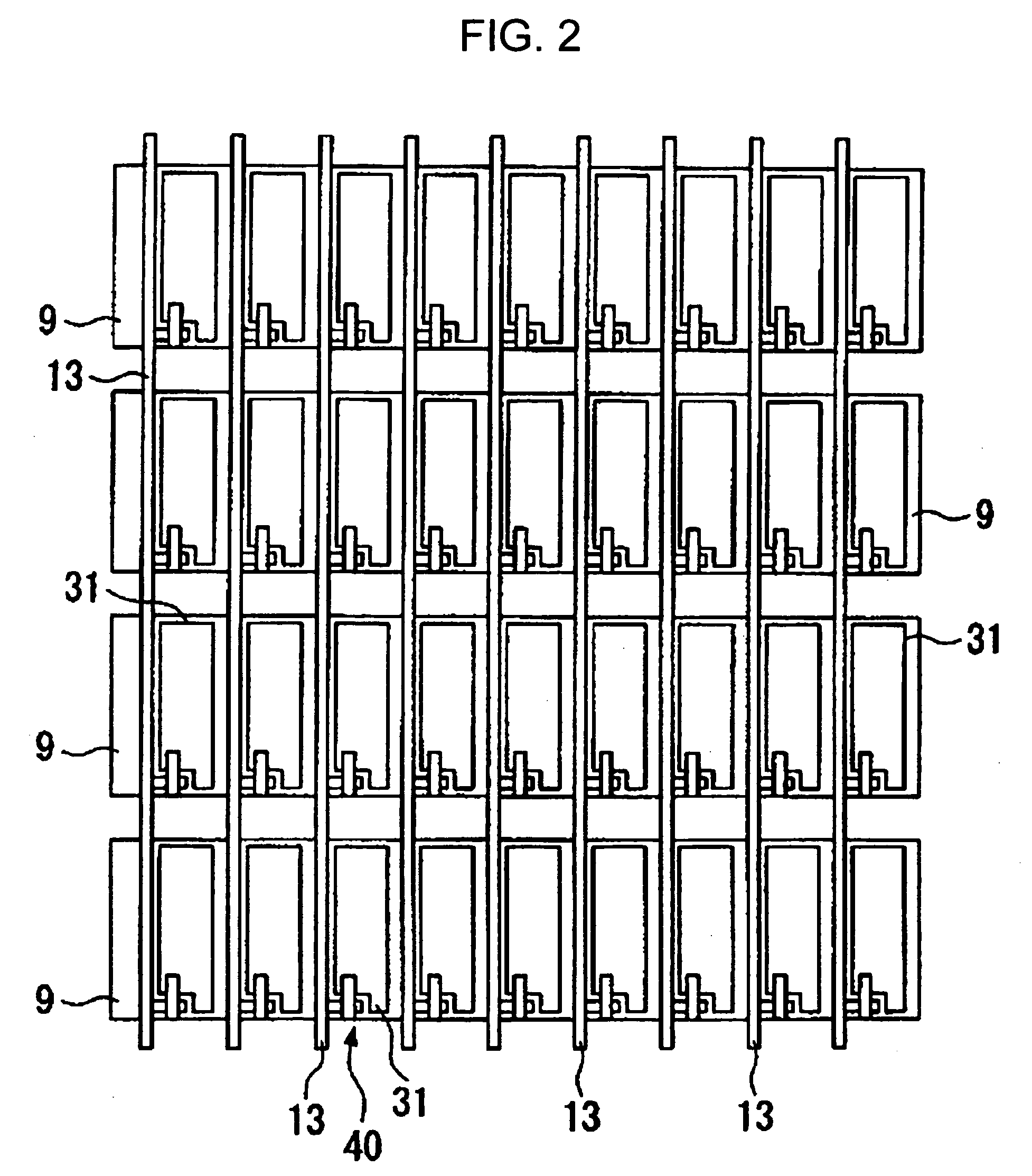
[0040] While referring to FIGS. 1 to 3, a first embodiment of the invention will be described. In the figures, each layer and each member are shown with sizes large enough to be seen, so that each layer and each member are shown using different scales.
[0041] A liquid crystal display device of the first embodiment described below is an active matrix liquid crystal display device using thin film diodes (hereunder abbreviated as “TFDs”) as switching elements, and is, in particular, a transflective liquid crystal display device which can provide a reflective display and a transmissive display.
[0042]FIG. 1 shows an equivalent circuit for a liquid crystal display device 100 according to the embodiment. The liquid crystal display device 100 includes a scanning signal drive circuit 110 and a data signal drive circuit 120. In the liquid crystal display device 100, signal lines, that is, a plurality of scanning lines 13 and a plurality of data lines 9 intersecting the scanning lines 13 are ...
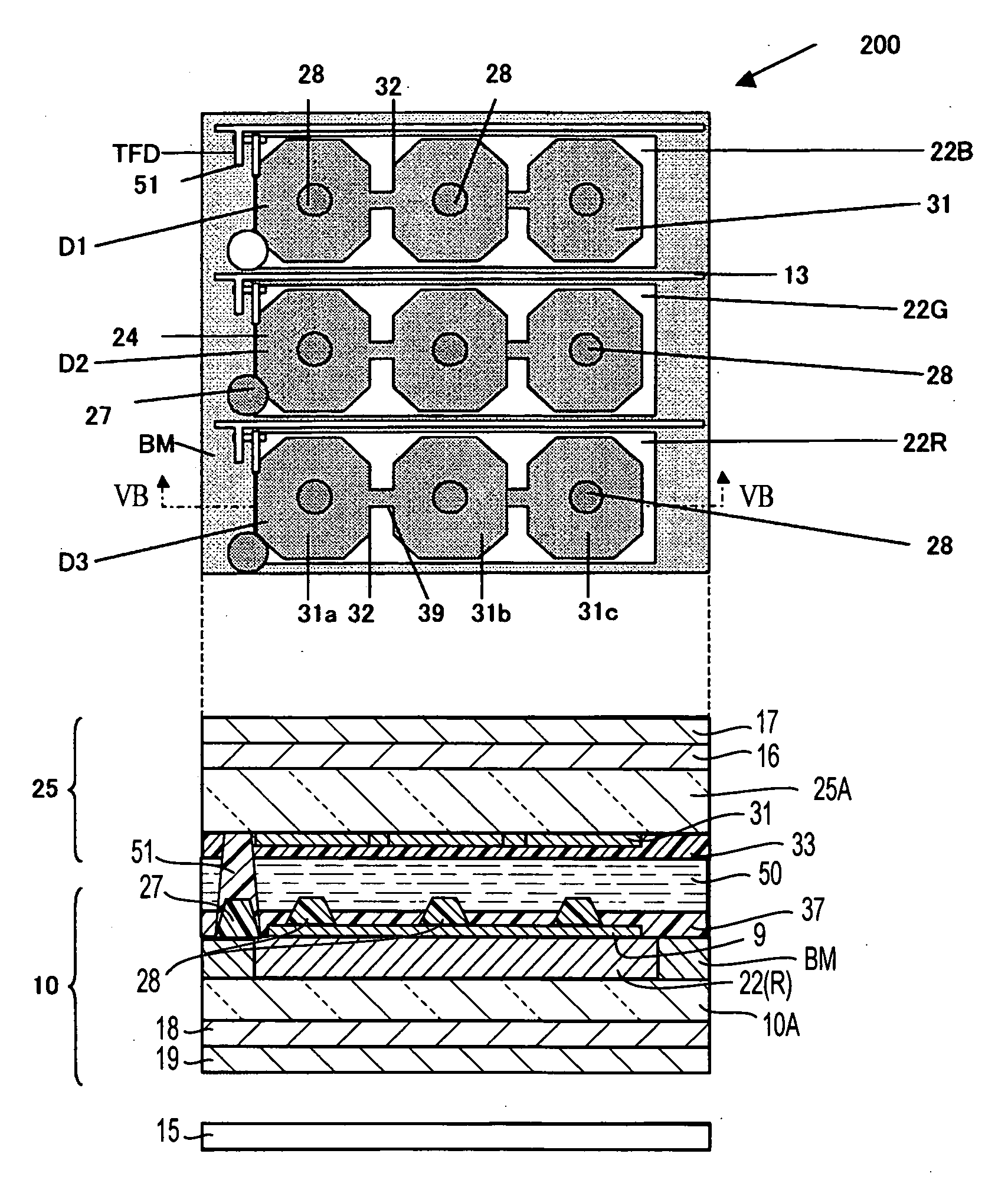
second embodiment
[0064] A second embodiment of the invention will be described with reference to FIGS. 4A and 4B.
[0065]FIGS. 4A and 4B are a plan view and a sectional view of a liquid crystal display device of the second embodiment, respectively, and are schematic views in correspondence with those of FIGS. 3A and 3B showing the first embodiment. Parts in the second embodiment corresponding to those in the first embodiment are given the same reference numerals.
[0066] A liquid crystal display device 200 according to the second embodiment is a transmissive liquid crystal display device which does not have a reflective display area. As shown in FIG. 4A, the liquid crystal display device 200 has dot areas including respective pixel electrodes 31 disposed inwardly of data lines 9, scanning lines 13, etc. In each dot area, one coloring layer for one of the three primary colors is disposed, so that pixel areas including respective coloring layers 22B (blue), 22G (green), and 22R (red) are formed at three...
third embodiment
[0079] A third embodiment of the invention will be described with reference to FIGS. 5A and 5B.
[0080]FIGS. 5A and 5B are a plan view and a sectional view of a liquid crystal display device of the third embodiment, respectively, and are schematic views in correspondence with those of FIGS. 3A and 3B showing the first embodiment. Parts in the third embodiment corresponding to those in the first embodiment are given the same reference numerals.
[0081] A liquid crystal display device 200 according to the third embodiment is a transmissive liquid crystal display device which does not have a reflective display area. As shown in FIG. 5A, the liquid crystal display device 200 has dot areas including respective pixel electrodes 31 disposed inwardly of data lines 9, scanning lines 13, etc. In each dot area, one coloring layer for one of the three primary colors is disposed, so that pixel areas including respective coloring layers 22B (blue), 22G (green), and 22R (red) are formed at three dot...
PUM
Abstract
A liquid crystaldisplay device includes a pair of opposing substrates; a liquid crystal layer disposed between the pair of substrates, the liquid crystal layer being formed of liquid crystal which has a negative dielectricanisotropy and which is vertically aligned in an initial alignment state; pixels disposed in a matrix within an area of one of the pair of substrates, each pixel including a pixel electrode, a gap between the pixel electrode of the pixel and the pixel electrode of an adjacent pixel, a switching element connected to the pixel electrode, and a metal line connected to the switching element, the pixels including a first pixel and a second; a columnar spacer that separates the opposing substrates, the spacer being disposed at a position of the first pixel that corresponds to the gap of the first pixel or in overlap with the switching element of the first pixel; and a first protrusion having a height that is less than the height of the spacer and that is disposed at a position of the second pixel that corresponds to the position of the first pixel where the spacer is disposed.
Description
BACKGROUND OF THE INVENTION [0001] 1. Technical Field [0002] The present invention relates to a liquid crystal display device and an electronic apparatus, and, more particularly, to a technology which provides a display having a wide viewing angle range and a high contrast in a liquid crystal display device using homeotropic liquid crystal. [0003] 2. Related Art [0004] A transflective liquid crystal display device having a reflection mode and a transmission mode is known as a liquid crystal display device. A transflective liquid crystal display device of a type in which a liquid crystal layer is disposed between an upper substrate and a lower substrate and a reflective film (a metallic film, such as an aluminum film, having a window for transmitting light) is disposed at the inner surface of the lower substrate and functions as a transflective plate has been proposed. In this case, in the reflection mode, incident outside light from the upper substrate passes through the liquid crys...
Claims
Application Information
Patent Timeline
Application Date:The date an application was filed.
Publication Date:The date a patent or application was officially published.
First Publication Date:The earliest publication date of a patent with the same application number.
Issue Date:Publication date of the patent grant document.
PCT Entry Date:The Entry date of PCT National Phase.
Estimated Expiry Date:The statutory expiry date of a patent right according to the Patent Law, and it is the longest term of protection that the patent right can achieve without the termination of the patent right due to other reasons(Term extension factor has been taken into account ).
Invalid Date:Actual expiry date is based on effective date or publication date of legal transaction data of invalid patent.

