Defect repair device and defect repair method

a technology of defect repair and repair device, which is applied in the direction of photomechanical treatment, photomechanical equipment, instruments, etc., can solve the problems of phase defect, degrade the optical properties of ml film, and produce a modulation of the phase of the reflected field

Inactive Publication Date: 2006-01-12
ASAHI GLASS CO LTD
View PDF13 Cites 47 Cited by
  • Summary
  • Abstract
  • Description
  • Claims
  • Application Information

AI Technical Summary

Benefits of technology

[0007] According to one aspect of the present invention, a defect repair device includes a defect inspection unit, a calculation unit, an energy supplier and an energy controller. The defect inspection unit is configured to find a size of a protruding defect on a front surface of a multi-layer film having a rear surface opposite to the front surface. The calculation unit is configured to calculate a repair energy so as to repair the protruding defect, based on the size of the protruding defect found by the defect inspection unit. The energy controller is configured to control the energy supplier to supply the repair energy calculated by the calculation unit to a portion in the multi-layer film from the rear surface of the multi-layer film so as to cause a decrease in a volume of the portion and retract the protruding defect into the multi-layer film.

Problems solved by technology

Among defects of a reticle or reflective mirrors, a phase defect is a type of defect that produces a modulation of the phase of the reflected field and is caused by the displacement of layers of the ML film due to the presence of a foreign object.
However, since the ML film absorbs the electron beam to some extent, and optical properties of the ML film are controlled by about 20 to 30 layers from the front surface of the ML film, the Barty et al. technique applying the electron beam from the front surface may degrade the optical properties of the ML film.

Method used


Image

  • Defect repair device and defect repair method
  • Defect repair device and defect repair method
  • Defect repair device and defect repair method

Examples


Embodiment Construction

[0019] The preferred embodiments will now be described with reference to the accompanying drawings, wherein like reference numerals designate corresponding or identical elements throughout the various drawings.

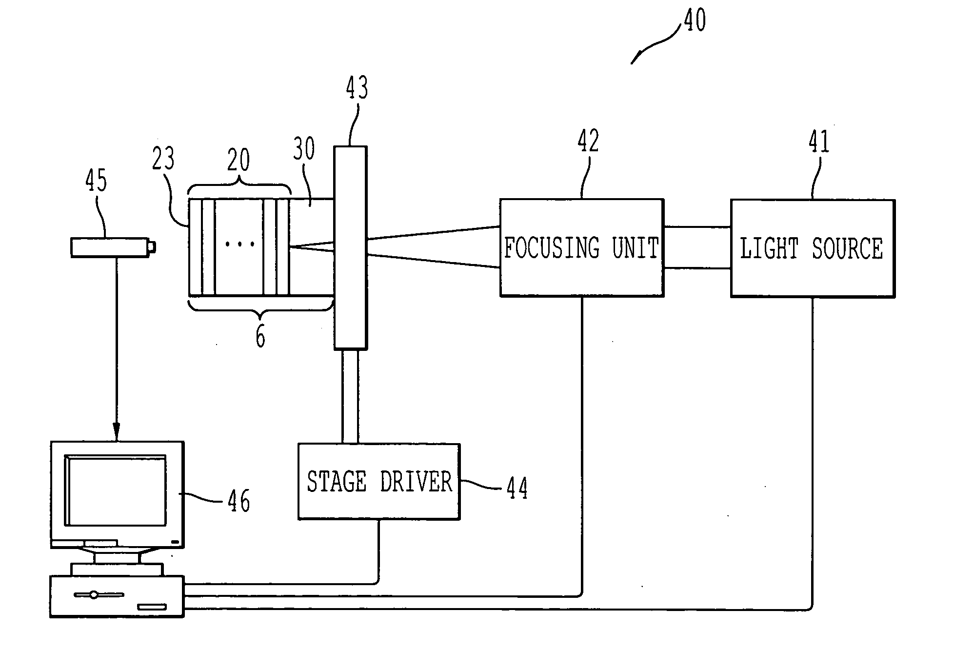
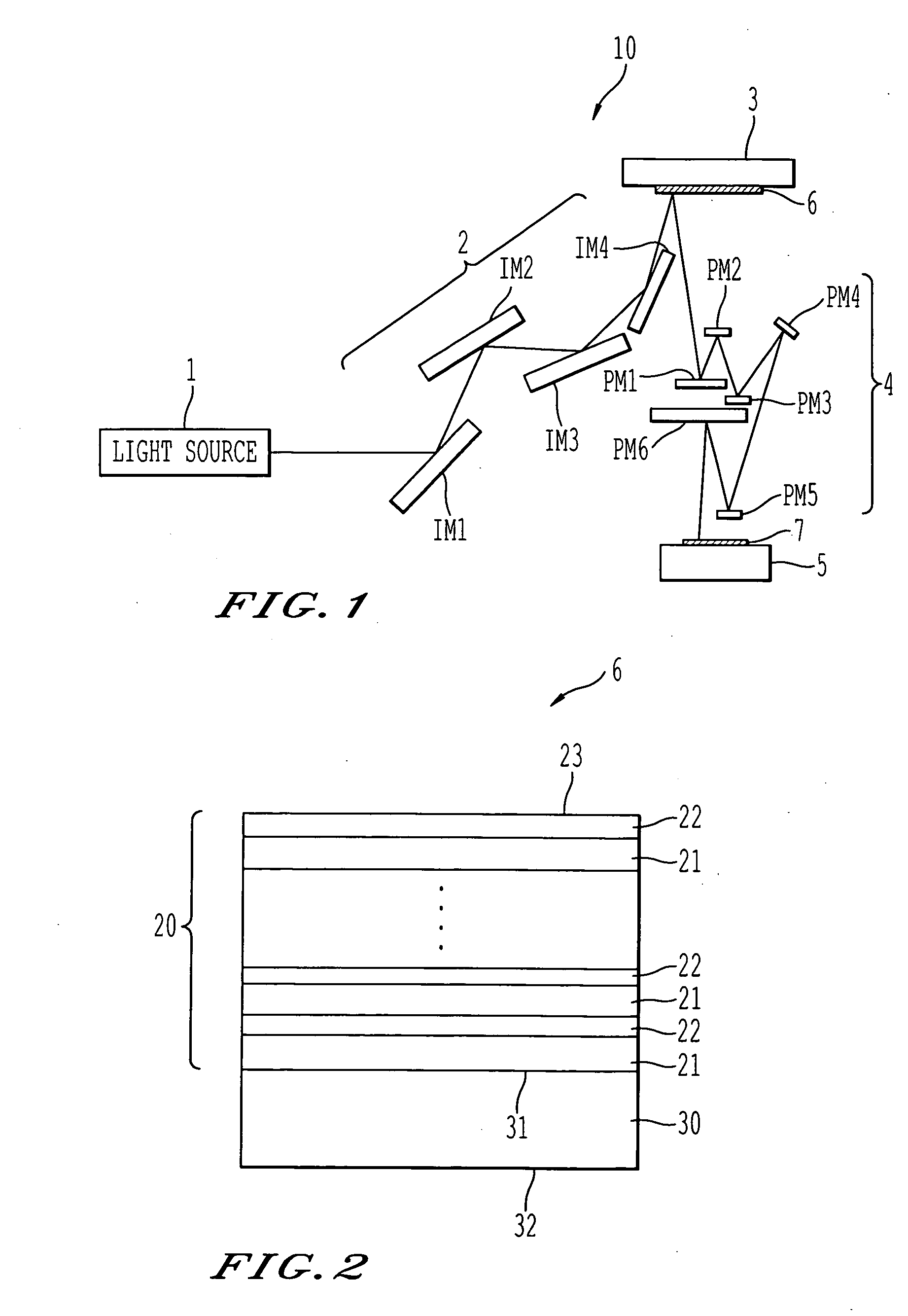
[0020]FIG. 1 is a schematic illustration of an exposure tool for extreme ultraviolet lithography (hereinafter, “EUVL”) utilizing extreme ultraviolet light (hereinafter, “EUV light”) as exposure light source. As shown in FIG. 1, an exposure tool 10 includes a light source 1, an illumination mirror unit 2, a reticle stage 3, a projection mirror unit 4 and a wafer stage 5. The light source 1 is configured to emit exposure light having a desired wavelength, for example, about 13 nm in EUVL. The illumination mirror unit 2 includes reflective mirrors IM1-IM4 each configured to reflect incident light, and the finally-reflected light reaches a reticle 6 provided on the reticle stage 3 and uniformly illuminates the reticle 6. The reticle 6 has a circuit pattern to be formed on a wafer...


PUM

PropertyMeasurementUnit
temperatureaaaaaaaaaa
wavelengthaaaaaaaaaa
full width at half maximumaaaaaaaaaa

Abstract

A defect repair device includes a defect inspection unit configured to find a size of a protruding defect on a front surface of a multi-layer film having a rear surface opposite to the front surface, a calculation unit configured to calculate a repair energy so as to repair the protruding defect based on the size of the protruding defect found by the defect inspection unit, an energy supplier, and an energy controller configured to control the energy supplier to supply the repair energy calculated by the calculation unit to a portion in the multi-layer film from the rear surface of the multi-layer film so as to cause a decrease in a volume of the portion and retract the protruding defect into the multi-layer film.

Description

BACKGROUND OF THE INVENTION [0001] 1. Field of the Invention [0002] The present invention relates to a defect repair device and a defect repair method. [0003] 2. Discussion of the Background [0004] In manufacturing semiconductor integrated circuits, an exposure tool is used to print fine circuit patterns on a reticle onto a wafer. In order to achieve higher integration and greater performance, integrated circuits are made to have even finer structures, and thus an exposure tool is required to print detailed circuit patterns on the wafer, obtaining a deep focal depth and high resolution. Accordingly, the use of exposure light with shorter wavelengths has been attempted. For example, exposure techniques using g-line, i-line, KrF excimer laser and ArF excimer laser have been developed, and their wavelengths are 436 nm, 365 nm, 248 nm and 193 nm, respectively. Among the light with even shorter wavelengths, there is extreme ultraviolet light (hereinafter, “EUV light”) having a wavelength...

Claims


Application Information

Patent Timeline
Patent Type & Authority Applications(United States)
IPC IPC(8): G01N21/00
CPCB82Y10/00B82Y40/00G03F1/0092G03F1/24G21K2201/067G03F1/84G03F7/70591G03F7/70958G21K1/062G03F1/72
Inventor IKUTA, YOSHIAKIUNO, TOSHIYUKI
Owner ASAHI GLASS CO LTD
Why Eureka
Try Eureka