Memory utilizing oxide-conductor nanolaminates

a technology of oxide-conducting nanolaminates and memory, which is applied in the direction of digital storage, instruments, transistors, etc., can solve the problems of poorly controlled thickness and structure that did not gain widespread acceptance and us

Inactive Publication Date: 2006-01-12
MICRON TECH INC
View PDF99 Cites 114 Cited by
  • Summary
  • Abstract
  • Description
  • Claims
  • Application Information

AI Technical Summary

Benefits of technology

[0050] The above mentioned problems for creating DRAM technology compatible floating gate transistor cells as well as other problems are addressed by the present invention and will be understood by reading and studying the following specifi

Problems solved by technology

However, these structures did not gain widespread acceptance and use due to their variability in characteristics and unpredictable charge trapping phenomena.
Sinc

Method used


Image

  • Memory utilizing oxide-conductor nanolaminates
  • Memory utilizing oxide-conductor nanolaminates
  • Memory utilizing oxide-conductor nanolaminates

Examples


Embodiment Construction

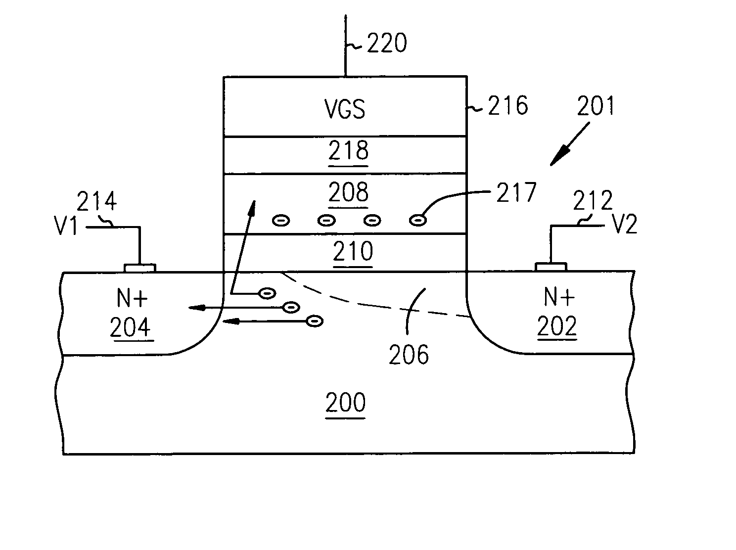
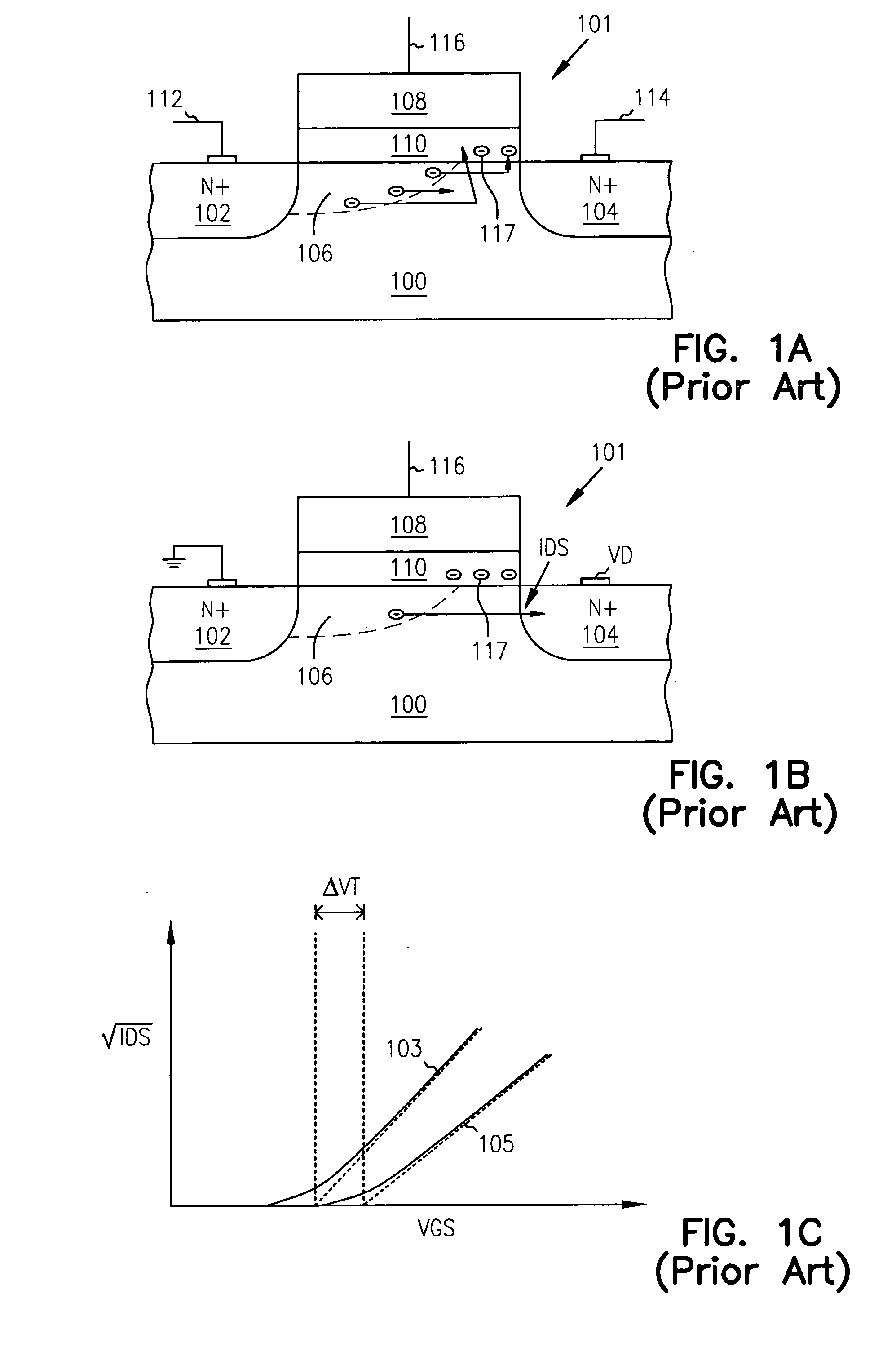
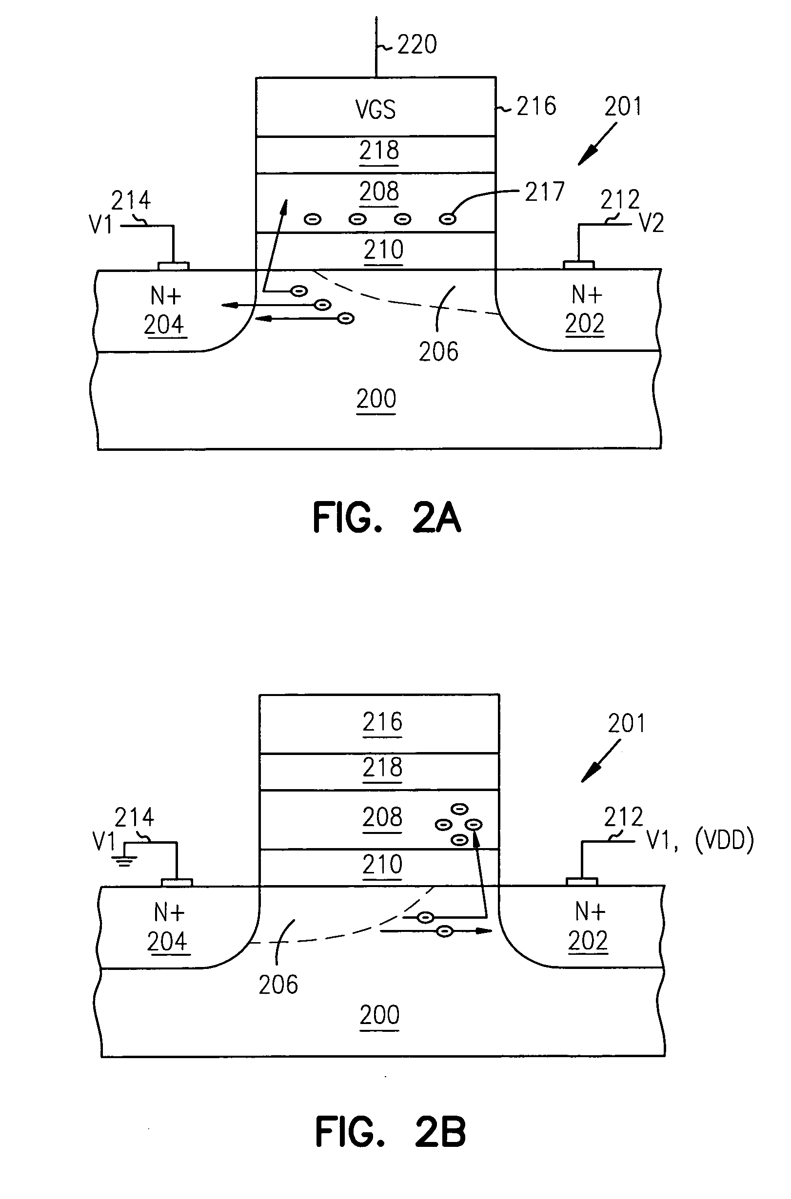
[0069] In the following detailed description of the invention, reference is made to the accompanying drawings which form a part hereof, and in which is shown, by way of illustration, specific embodiments in which the invention may be practiced. In the drawings, like numerals describe substantially similar components throughout the several views. These embodiments are described in sufficient detail to enable those skilled in the art to practice the invention. Other embodiments may be utilized and structural, logical, and electrical changes may be made without departing from the scope of the present invention.

[0070] The terms wafer and substrate used in the following description include any structure having an exposed surface with which to form the integrated circuit (IC) structure of the invention. The term substrate is understood to include semiconductor wafers. The term substrate is also used to refer to semiconductor structures during processing, and may include other layers that...


PUM


Abstract

Structures, systems and methods for floating gate transistors utilizing oxide-conductor nanolaminates are provided. One floating gate transistor embodiment includes a first source/drain region, a second source/drain region, and a channel region therebetween. A floating gate is separated from the channel region by a first gate oxide. The floating gate includes oxide-conductor nanolaminate layers to trap charge in potential wells formed by different electron affinities of the oxide-conductor nanolaminate layers.

Description

CROSS REFERENCE TO RELATED APPLICATIONS [0001] The present application is a divisional of U.S. application Ser. No. 10 / 191,336, filed Jul. 8, 2002, which is incorporated herein by reference in its entirety. [0002] This application is related to the following co-pending, commonly assigned U.S. patent applications: “Memory Utilizing Oxide Nanolaminates,” Ser. No. 10 / 190,717, filed Jul. 8, 2002; and “Memory Utilizing Oxide-Nitride Nanolaminates,” Ser. No. 10 / 190,689, filed Jul. 8, 2002; each of which disclosure is herein incorporated by reference.FIELD OF THE INVENTION [0003] The present invention relates generally to semiconductor integrated circuits and, more particularly, to memory utilizing oxide-conductor nanolaminates. BACKGROUND OF THE INVENTION [0004] Many electronic products need various amounts of memory to store information, e.g. data. One common type of high speed, low cost memory includes dynamic random access memory (DRAM) comprised of individual DRAM cells arranged in ar...

Claims


Application Information

Patent Timeline
IPC IPC(8): H01L21/8238G11C11/56G11C16/04H01L27/115H01L29/423H01L29/788
CPCG11C11/5671G11C16/0416H01L29/7885H01L29/42332H01L27/115H10B69/00
Inventor FORBES, LEONARDAHN, KIE Y.
Owner MICRON TECH INC
Why Eureka
Try Eureka