RF device on insulating substrate and method of manufacturing RF device

a technology of insulating substrate and rf device, which is applied in the direction of substation equipment, electrical equipment, antennas, etc., can solve the problems of low durability, low reliability of the junction between these components, and separate rf devices, and achieves the effects of low cost, excellent durability, and communication capability

Inactive Publication Date: 2006-01-12
NEC CORP
View PDF10 Cites 151 Cited by
  • Summary
  • Abstract
  • Description
  • Claims
  • Application Information

AI Technical Summary

Benefits of technology

[0024] It is an object of the present invention to provide an RF device which has excellent durability, communication capability, and appearance and which can be manufactur

Problems solved by technology

The separate-type RF device is problematic in that they are of low durability.
Specifically, since the separate-type RF device is of such a structure that an IC chip mounted on a substrate with an antenna disposed thereon, junctions between these components are not highly reliable.
Therefore, the RF tags are liable to undergo thermal stresses, which tend to break the junctions between the components thereof.
The junctions between the components of RF tags can also be broken when products with the RF tags attached thereto are vibrated or shocked during shipment or when the RF tags are subjected to bending stresses while being applied to clothes or paper products.
Actually, an introduction test conducted on conventional separate-type RF tags reported that they had a failure rate of nearly 10%.
Separate-type RF devices are highly costly to manufacture.
However, smaller-size IC chips are likely to suffer an increase in the cost of mounting them.
In view of the yield and other factors, it is a task that cannot easily be achieved to reduce the manufacturing cost of separate-type RF devices.
Another drawback of separate-type RF devices is that when they are incorporated in IC cards, they have a poor appearance.
Attempts to improve the appearance tend to incur expenses.
Specificall

Method used


Image

  • RF device on insulating substrate and method of manufacturing RF device
  • RF device on insulating substrate and method of manufacturing RF device
  • RF device on insulating substrate and method of manufacturing RF device

Examples


first embodiment

[0060] An RF device according to the present invention will first be described below.

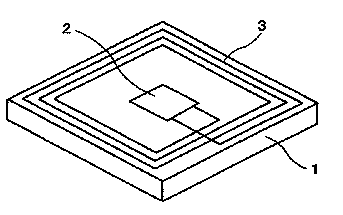
[0061] As shown in FIG. 4, the RF device according to the first embodiment of the present invention has insulating substrate 1 supporting rectangular signal processing circuit 2 and spiral antenna 3 that are integrally formed thereon. Insulating substrate 1 may comprise a glass substrate or a plastic substrate. In the illustrated embodiment, insulating substrate 1 comprises a glass substrate. Antenna 3 comprises a single wire wound in a rectangular spiral pattern. Generally, RF tag systems for use in a 13.56 Hz frequency band operate on the principle of electromagnetic induction for the RF tag to obtain electromotive forces from radio waves. Antenna 3 has opposite terminals connected to one side of rectangular signal processing circuit 2 that is disposed centrally on the surface of insulating substrate 1. Antenna 3 has an outermost pattern edge disposed along the outer profile edge of insulating sub...

second embodiment

[0115] A first modification of the present invention will be described below.

[0116] In the second embodiment described above, antenna 3 is formed by electrolytic plating as shown in FIGS. 10A through 10C. According to the first modification of the second embodiment, antenna 3 is formed by electroless plating as shown in FIGS. 11A and 11B. As shown in FIG. 11A, base film 61 which serves as a base for selectively growing an electrolessly plated film is formed on the entire surface of insulating substrate 1 by sputtering, for example. Then, base film 61 is patterned to the shape of antenna 3 by photolithography. Base film 61 is formed of aluminum or nickel, for example. Then, as shown in FIG. 11B, plated film 62 is formed on base film 61 by electroless plating. At this time, plated film 62 is selectively formed on base film 61. Plated film 61 is formed of nickel, copper, or gold, for example. Other details of the first modification of the second embodiment are identical to those of the...

third embodiment

[0123] First, an RF device according to the present invention will be described below.

[0124] In the first embodiment described above, only signal processing circuit 2 is disposed centrally on insulating substrate 1, as shown in FIG. 4. According to the third embodiment, as shown in FIG. 13, signal processing circuit 2 and memory circuit 81 are disposed adjacent to each other centrally on insulating substrate 1.

[0125] Memory circuit 81 comprises a ROM for storing information of an RF tag in advance and a DRAM or an SRAM for reading and writing information at the time of signal processing. The ROM, the DRAM, and the SRAM are fabricated by the process of manufacturing a CMOS according to the second embodiment described above. Other structural details of the third embodiment are identical to those of the first embodiment described above.

[0126] In the third embodiment, since memory circuit 81 is integrally disposed on the glass substrate on which signal processing circuit 2 and antenna...


PUM


Abstract

An RF device which has excellent durability and communication capability, and which can be manufactured at a low cost, and a method of manufacturing such an RF device are disclosed. The RF device has an insulating substrate for blocking radio waves and preventing noise from being produced. The RF device also has a signal processing circuit formed on the insulating substrate so that it does not need junctions which would be formed by a mounting process. An antenna is integrally formed with the signal processing circuit on the insulating substrate, and is connected to the signal processing circuit.

Description

BACKGROUND OF THE INVENTION [0001] 1. Field of the Invention [0002] The present invention relates to an RF device having an antenna and a signal processing circuit, for handling tag information, sensor information, security information, etc., a method of manufacturing such an RF device, a method of inspecting such an RF device, an RF apparatus, and a method of manufacturing such an RF apparatus. [0003] 2. Description of the Related Art [0004] Recently, RF (Radio-Frequency) devices such as RF tags or noncontact IC cards are quickly being put to practical use. RF tags comprise an antenna, a memory, and a signal processing circuit, and tag information stored in the memory is transmitted to and from a dedicated reader / writer for merchandise management and security control. [0005] As shown in FIG. 1 of the accompanying drawings, an RF tag has antenna 302 mounted on substrate 301 and IC chip 303 mounted on substrate 301 in electrical connection to antenna 302. Substrate 301 is usually mad...

Claims


Application Information

Patent Timeline
IPC IPC(8): H04M1/00
CPCH01Q1/22H01Q7/00H01Q1/38
Inventor NODA, SHUNJIKANOH, HIROSHI
Owner NEC CORP
Why Eureka
Try Eureka