

Light emitting element
a technology of light-emitting elements and light-emitting components, which is applied in the direction of transportation and packaging, thermoelectric devices, other domestic articles, etc., can solve the problems of more and more limited choices, and achieve the effect of suppressing color purity and luminous efficiency
- Summary
- Abstract
- Description
- Claims
- Application Information
AI Technical Summary
Benefits of technology
Problems solved by technology
Method used
Image

Examples
embodiment mode 1
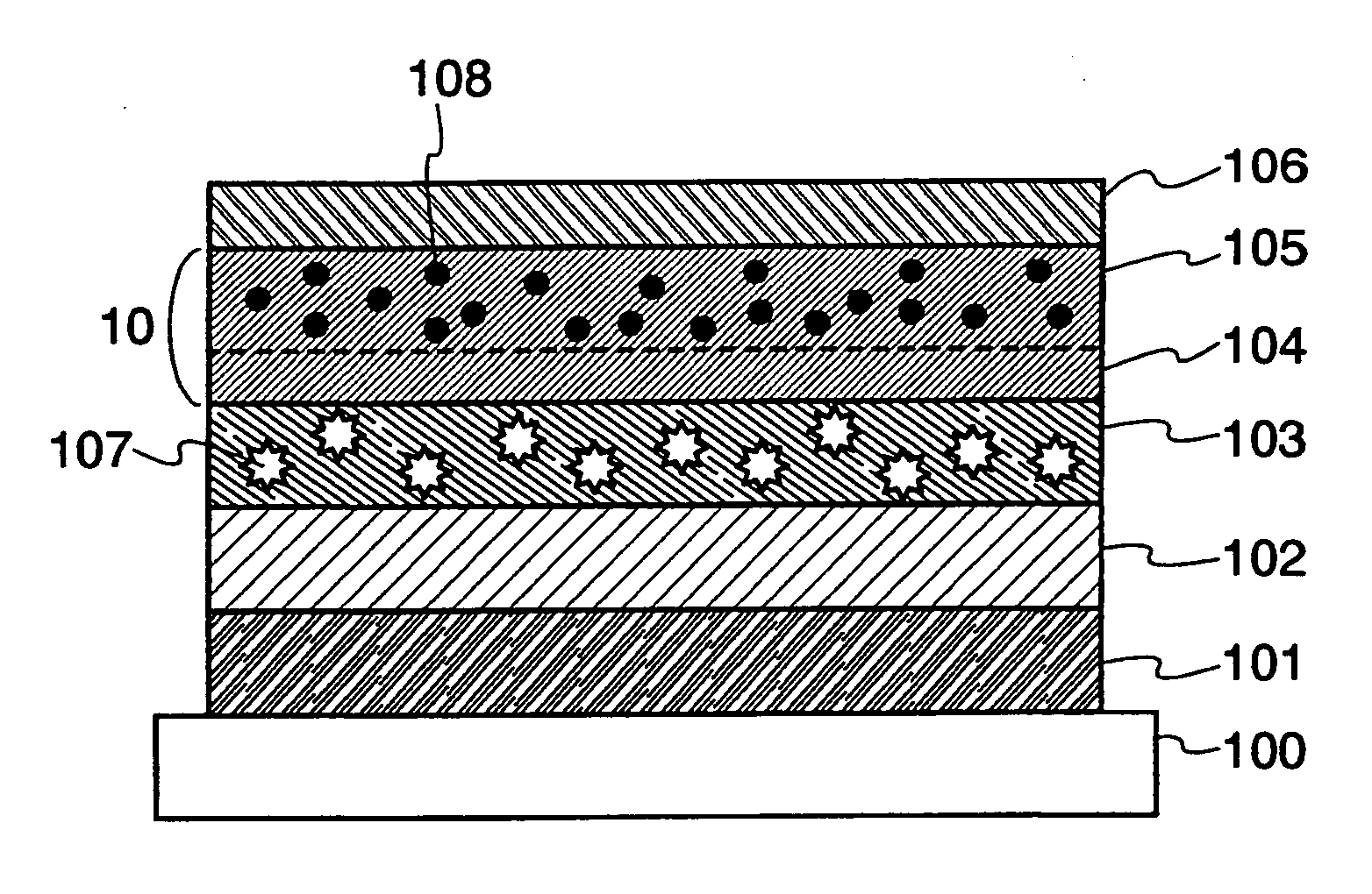
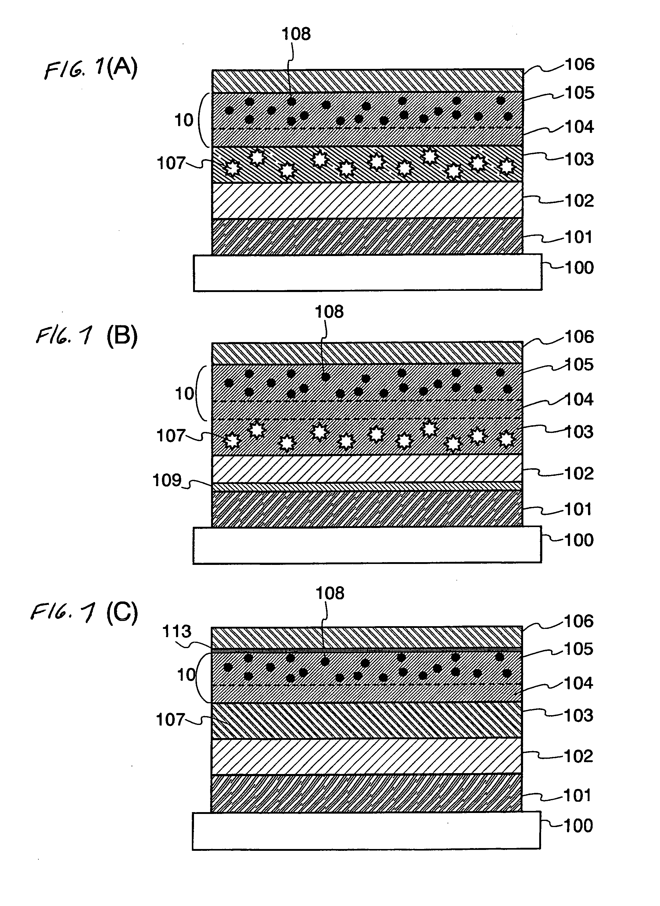
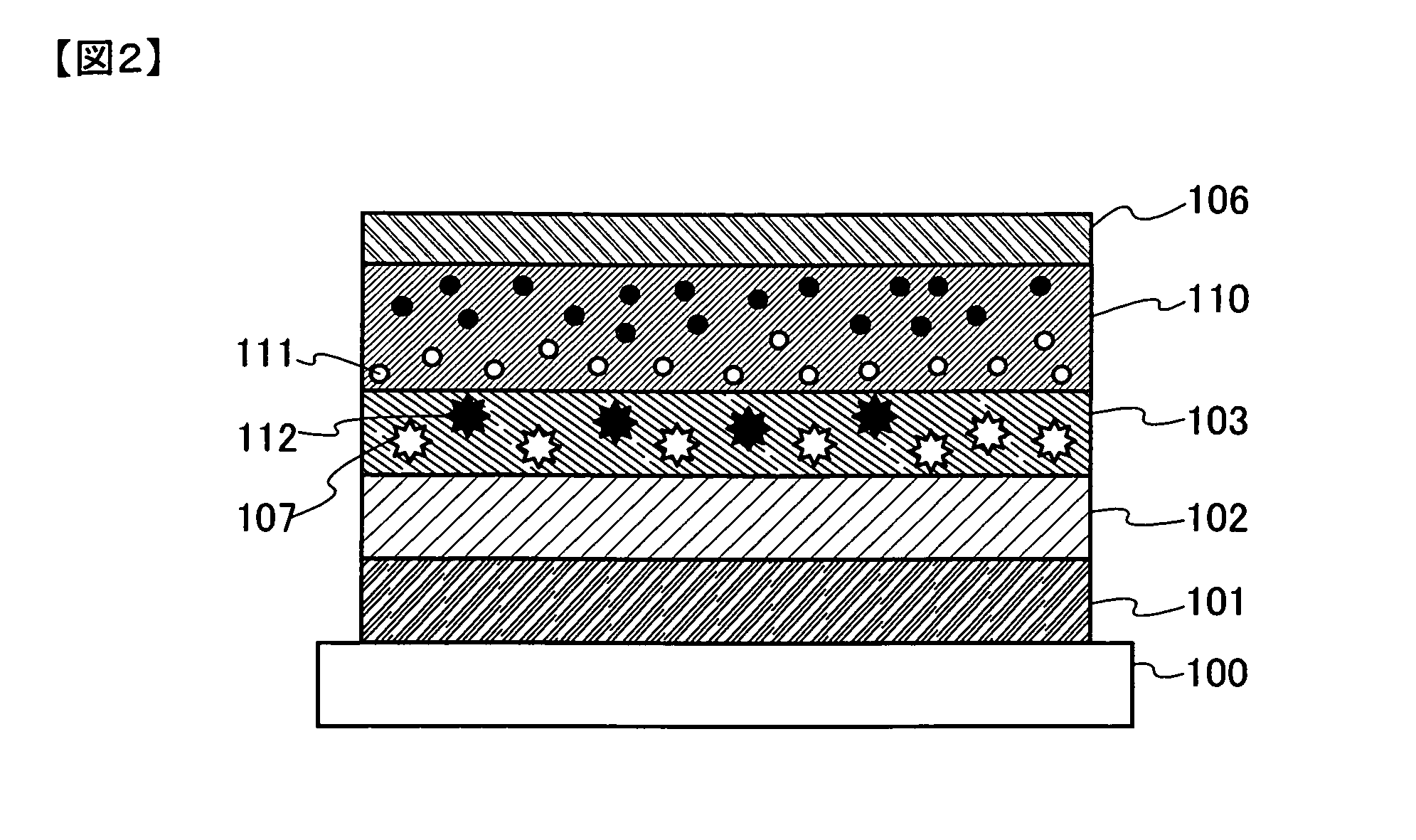
[0034]FIG. 1(A) shows one example of a structure of a thin film light emitting element according to the present invention. A thin film light emitting element according to the present embodiment mode includes an anode 101, a hole transporting layer 102, a light emitting layer 103 containing luminescent substances 107, an electron transporting layer 10 and a cathode 106 that are formed over an insulating surface of a substrate 100 or the like. The electron transporting layer 10 is divided into two layer regions, and at least one common electron transporting material is used in the two regions. Of the two regions, a first region 105 that is closer to the cathode 106 is doped with additives 108 in addition to the electron transporting material to improve the electron transporting property, the electron injecting property or both thereof, whereas a second region 104 that is closer to the light emitting layer 103 is not doped with the additives 108.
[0035] It is to be noted that the first...
embodiment mode 2
[0048] In the present embodiment mode, a method for manufacturing a display device according to the present invention will be described with reference to FIGS. 3 and 4. It is to be noted that an example of manufacturing an active matrix type display device is described in the present embodiment mode; however, a thin film light emitting element according to the present invention can also be applied to a passive matrix type display device as a matter of course.
[0049] First, after a first base insulating layer 51a and a second base insulating layer 51b are formed over a substrate 50, a semiconductor layer is fuirther formed over the second base insulating layer 51b. (FIG. 3(A))
[0050] As a material for the substrate 50, glass, quartz, plastic (polyimide, acryl, polyethylene terephthalate, polycarbonate, polyacrylate, polyethersulfone and the like) and the like that have light-transmitting property can be used. These substrates may be polished to be used by CMP or the like if necessary...
embodiment mode 3
[0102] In the present embodiment mode, the appearance of a panel of a light emitting device corresponding to one mode of the present invention will be described with reference to FIGS. 6(A) to 6(B). FIG. 6(A) is a top view of a panel in which a transistor and a light emitting element that are formed over a substrate are sealed with a sealing material that is formed between the substrate and a counter substrate 4006. FIG. 6(B) is a cross-sectional view of FIG. 6(A). In addition, a structure of the light emitting element that is mounted in the panel is as follows: the light emitting element includes an anode, a hole transporting layer, a light emitting layer containing a luminescent substance, an electron transporting layer and a cathode; the electron transporting layer is divided into two layer regions; a first region that is closer to the cathode is doped with additives containing a polycyclic condensed ring and a second region that is closer to the light emitting layer is not doped...
PUM
| Property | Measurement | Unit |
|---|---|---|
| Thickness | aaaaa | aaaaa |
| Thickness | aaaaa | aaaaa |
| Electric potential / voltage | aaaaa | aaaaa |
Abstract
Description
Claims
Application Information