Film bulk acoustic resonator package and method of fabricating same

Inactive Publication Date: 2006-01-19
AVAGO TECH INT SALES PTE LTD
View PDF25 Cites 57 Cited by
  • Summary
  • Abstract
  • Description
  • Claims
  • Application Information

AI Technical Summary

Benefits of technology

[0006] Generally, embodiments of the present disclosure pertain to a microfabricated device having a film bulk acoustic resonator (FBAR) and a circuit packaged between a pair of bonded substrates. The FBAR device is located on one of the substrates, and the circuit is located on the other. The circuit is electrically connected to the FBAR device. Mounting the FBAR device and the circuit on the respective substrat

Problems solved by technology

The GaAs substrate used in the RF power amplifier packages is typically much more expensive than the Si substrate used in the FBAR packages.
Further, the techniques used

Method used


Image

  • Film bulk acoustic resonator package and method of fabricating same
  • Film bulk acoustic resonator package and method of fabricating same
  • Film bulk acoustic resonator package and method of fabricating same

Examples


Embodiment Construction

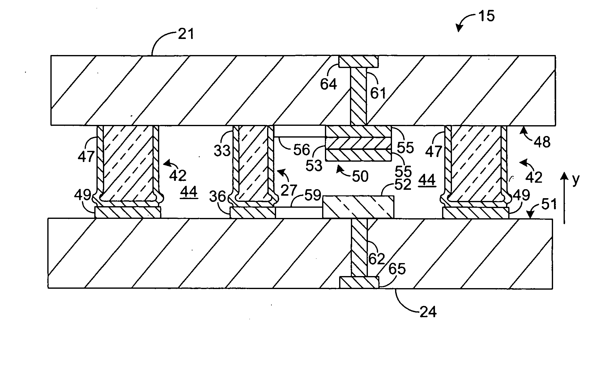
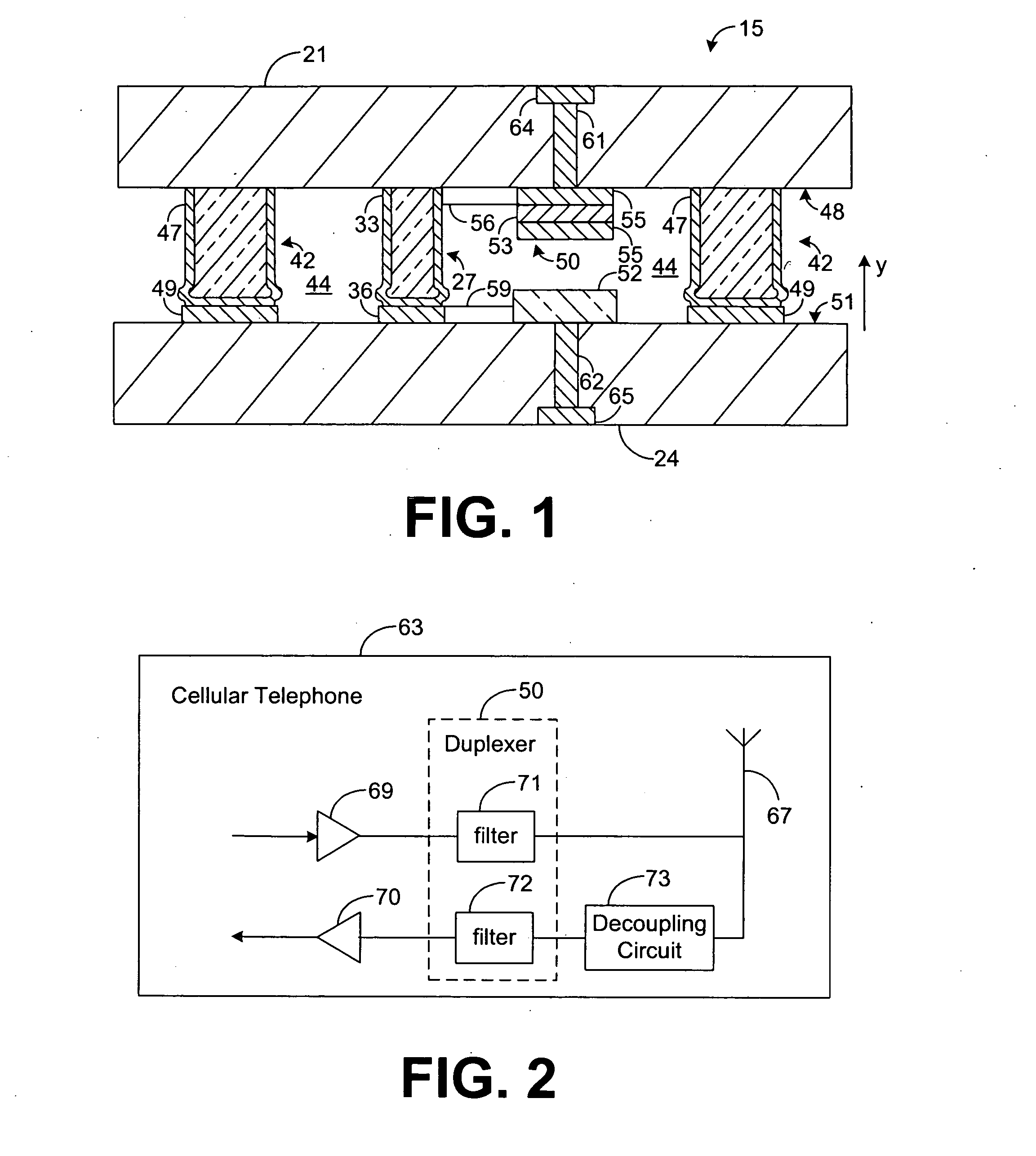
[0021] The present invention is based on the inventors' realization that the miniature FBAR package, efficient as it is, contains unused area, namely, the lid substrate, that could be used to mount other components. Moreover, in a conventional FBAR package, the material of the lid substrate is a semiconductor, so active devices can be fabricated in and on the lid substrate and can be located inside the chamber that also houses the FBAR device. The inventors have realized that, by locating the FBAR device on the lid substrate, and using GaAs as the material of the base substrate, the power amplifier can be fabricated on the base substrate while the FBAR device is fabricated on the lid substrate. The output of the power amplifier can be electrically connected directly to the transmitter port of the FBAR duplexer. With this structure, the FBAR device and the power amplifier occupy a common area of the main printed circuit board, which makes the printed circuit board area formerly occup...


PUM


Abstract

A microfabricated device has a first substrate, a second substrate, a film bulk acoustic resonator (FBAR) device, and a circuit. The second substrate is bonded to the first substrate to define a chamber. The FBAR device is located on a surface of the first substrate and inside the chamber. The circuit is located on a surface of the second substrate and inside the chamber. An electrical connection connects the circuit and the FBAR device.

Description

RELATED ART [0001] Film bulk acoustic resonator (FBAR) devices, such as FBAR-based duplexers used in mobile telephones and other mobile devices with radio frequency (RF) transmitters, are currently fabricated on a silicon (Si) substrate. An FBAR device is hermetically sealed inside a special miniature package composed of a base Si substrate on which FBARs are fabricated, a lid Si substrate covering the base substrate and a gasket between the substrates. The FBAR device package provides a very high packaging efficiency (volume ratio of the naked FBAR device to the packaged FBAR device). The FBAR device package is in turn mounted on a small but significant area of the main printed circuit board of the mobile telephone. [0002] Mobile telephones and other RF devices have a separately-packaged RF power amplifier that typically employs high electron mobility transistors (HEMTs) built in and on a gallium arsenide (GaAs) substrate. The RF power amplifier package is mounted on another small ...

Claims


Application Information

Patent Timeline
IPC IPC(8): H01L21/48H01L23/52
CPCH03B5/326H03H3/02H03H9/706H03H9/105H03H9/0547
Inventor LARSON,, JOHN D. IIIBAI, QINGMATTA, FARIDVERHOEVEN, TRACY
Owner AVAGO TECH INT SALES PTE LTD
Why Eureka
Try Eureka