

Plasma display panel
a technology of plasma display panel and display panel, which is applied in the direction of gas discharge electrodes, gas discharge vessels/containers, gas-filled discharge tubes, etc., can solve the problems of increasing electric power consumption, achieve the effect of improving the efficiency of light emission, and increasing the electric filing strength
- Summary
- Abstract
- Description
- Claims
- Application Information
AI Technical Summary
Benefits of technology
Problems solved by technology
Method used
Image

Examples
second embodiment
[0064]FIG. 4 is a front view illustrating a second embodiment of a PDP according to the present invention.
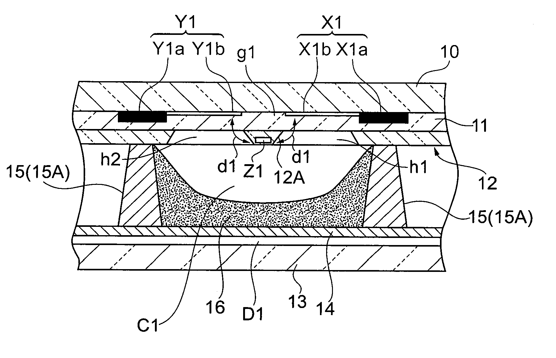
[0065] The first embodiment has described a PDP having the floating electrodes Z1 each formed in an isolated-island form independently in each discharge cell C1, whereas the PDP described in the second embodiment has floating electrodes Z2 each formed in the additional dielectric layer 12 in a strip shape extending in the row direction through the protuberances 12A each formed in the portion opposite the discharge gap g1 between the transparent electrodes X1b, Y1b.
[0066] The structure of the other components in this PDP is approximately the same as that in the first embodiment, and in FIG. 4 the same components are designated with the same reference numerals as those in the first embodiment.
[0067] As in the case of the PDP in the first embodiment, in the PDP in the second embodiment the dielectric-formed protuberance 12A extending out into the interior of the discharge cell C...
third embodiment
[0068]FIGS. 5 and 6 illustrate a third embodiment of the PDP according to the present invention. FIG. 5 is a schematic front view of the PDP in the third embodiment. FIG. 6 is a sectional view taken along the V2-V2 line in FIG. 5.
[0069] The first and second embodiments have described a PDP having the column electrodes D1 formed on the back glass substrate 13, whereas the PDP in the third embodiment as shown in FIGS. 5 and 6 has column electrodes D2 formed on the back-facing face of the front glass substrate 10.
[0070] More specifically, the dielectric layer 11 covers the row electrode pairs (X1, Y1), and each of the column electrodes D2 extends in the column direction on a portion of the back-facing face of the dielectric layer 11 opposite a mid-area between adjacent transparent electrodes X1b (Y1b) arranged at regular intervals along the associated bus electrodes X1a (Y1a) of the row electrode pairs (X1, Y1). The column electrodes D2 are covered by the additional dielectric layer ...
PUM
 Abstract
Description
Claims
Application Information