Multi-electron beam exposure method and apparatus

a multi-electron beam and exposure method technology, applied in the field of multi-electron beam exposure method and apparatus, can solve problems such as failure to prevent the size of equipment from being increased

Inactive Publication Date: 2006-01-26
HITACHI HIGH-TECH CORP
View PDF5 Cites 16 Cited by
  • Summary
  • Abstract
  • Description
  • Claims
  • Application Information

AI Technical Summary

Benefits of technology

[0015] The object of the present invention is to avoid the problems with systematization in such a multi-beam approach, and to provide a multi-electron beam exposure method and apparatus that can be realized by bit map data generation means of practical level.

Problems solved by technology

One of the problems in achieving the aforementioned exposure method is the pattern data generation method for controlling irradiation of each electron beam in conformity to a predetermined writing speed.
However, this requires an extra-high speed storage circuit having a massive capacity of as much as 2400 Giga-Bytes that stores the pattern having a maximum of about 25 mm square.
However, these proposals fail to prevent the size of the equipment from being increased due to the aforementioned reasons.

Method used


Image

  • Multi-electron beam exposure method and apparatus
  • Multi-electron beam exposure method and apparatus
  • Multi-electron beam exposure method and apparatus

Examples


Embodiment Construction

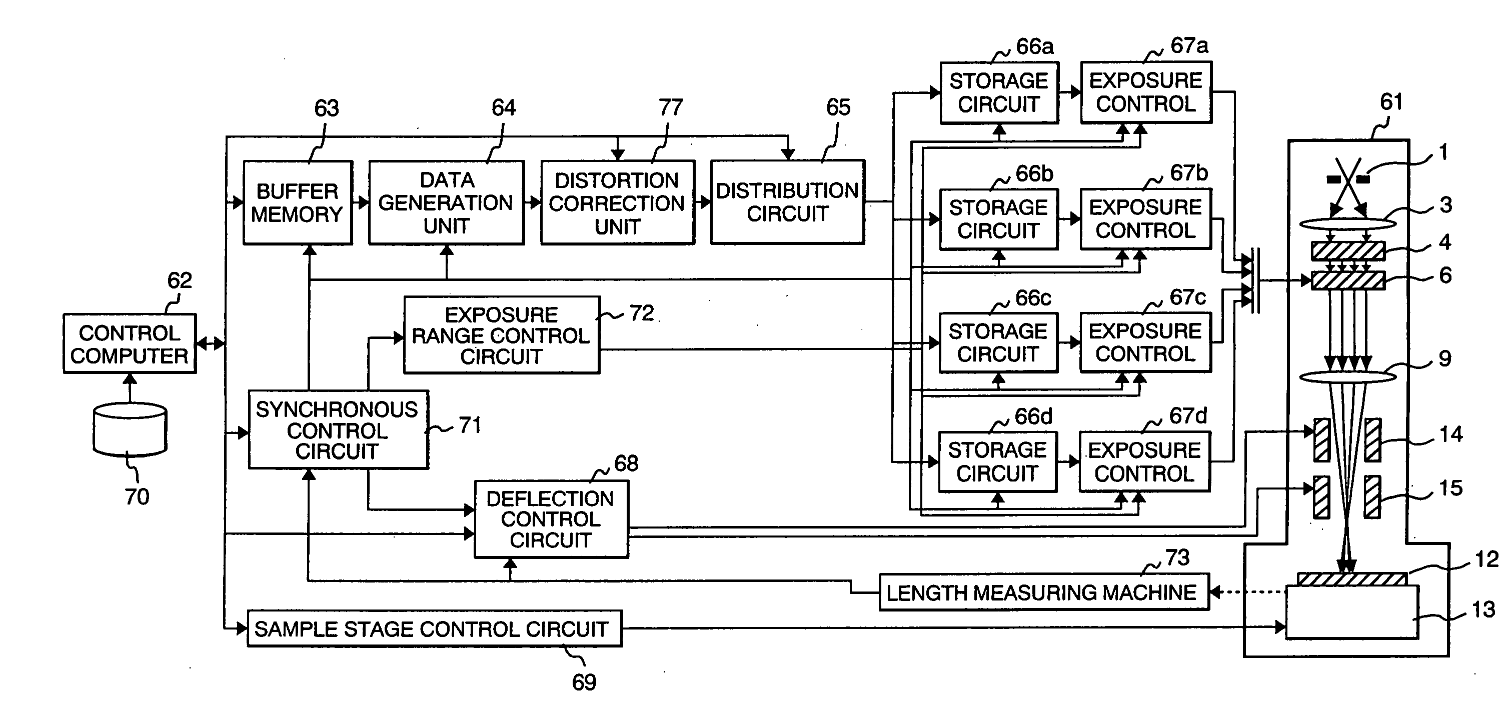
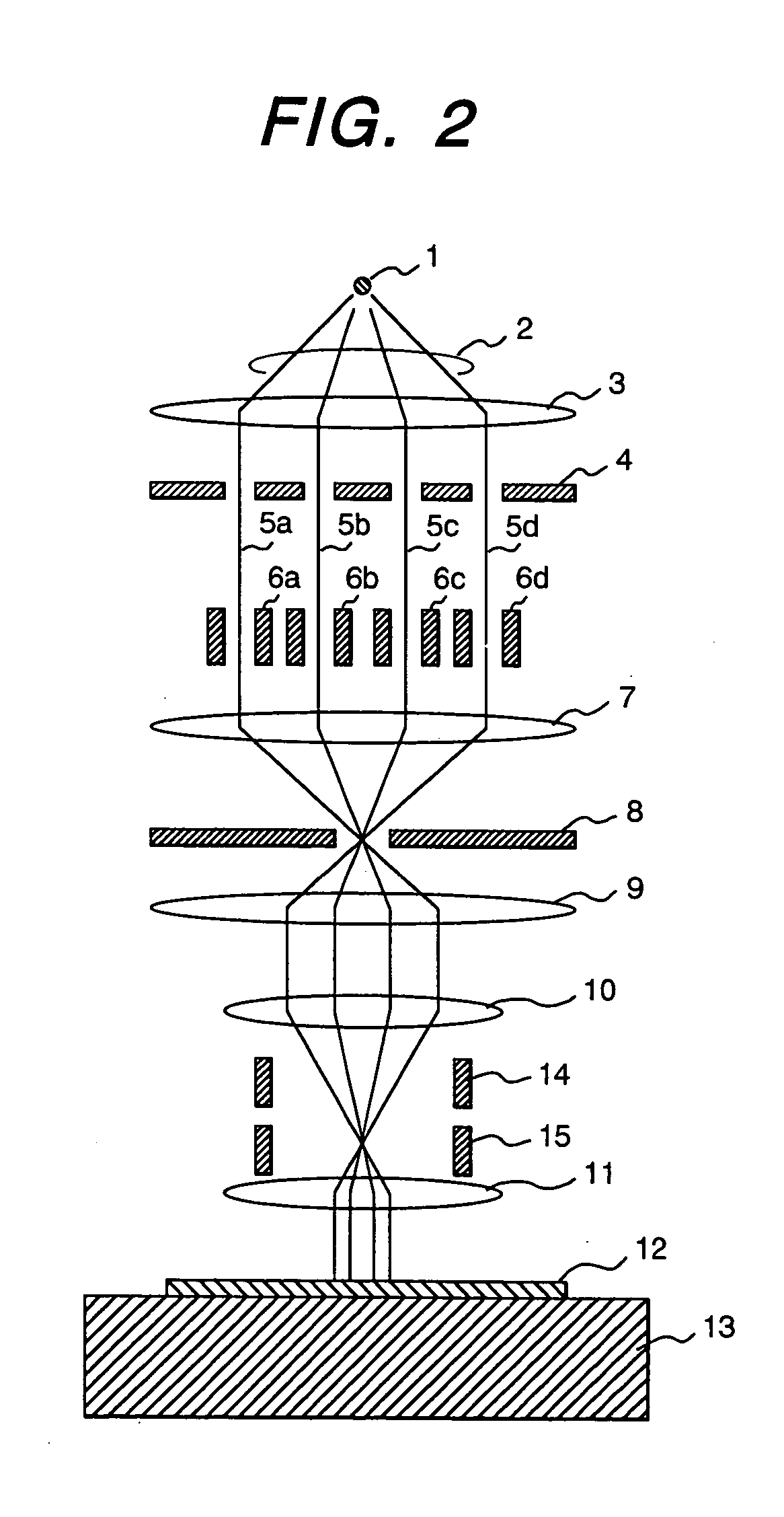
[0050] Referring to the drawings, the following describes the details of the preferred embodiments of the present invention: FIG. 2 shows an electron beam column for forming multiple spot beams. Electron beam 2 emitted from an electron gun 1 are corrected into parallel electron beams by an electron lens 3, and are partitioned into multiple electron beams 5a, 5b, 5c and 5d by an aperture array 4. The partitioned electron beams each pass through individual blanking deflectors 6a, 6b, 6c and 6d, and are converged by an electron lens 7 to pass through a blanking aperture 8.

[0051] Further, they are reduced by electron lens 9, 10 and 11, and are projected on the semiconductor 12 of a sample stage 13 as multiple spot beams. A main deflector 14 and sub-deflector 15 deflect the orbit of electron beam, thereby ensuring that the position exposed to electron beam on the semiconductor wafer 12 can be changed to any desired position within the range of deflection.

[0052] The time for each electr...


PUM

PropertyMeasurementUnit
widthaaaaaaaaaa
widthsaaaaaaaaaa
sizeaaaaaaaaaa

Abstract

A multi-electron beam exposure method and apparatus, wherein electron beams are applied to a sample surface mounted on a traveling sample stage to perform repeated exposure of chip patterns. An exposure region of the sample surface is partitioned into multiple stripe regions having a width in an x-axis direction, and each of the multiple stripe regions is further partitioned into multiple main fields having a width in a y-axis direction. At least one of the widths of the main fields in the x- and y-axis directions is set to a value, and exposure pattern data for one chip based on the partitioned main fields is stored as a unit. The stored exposure pattern data is readout a number of times corresponding to the number of chips repeatedly, and each electron beam provides repeated exposure of same regions of the chips.

Description

CROSS REFERENCE TO RELATED APPLICATIONS [0001] This application is a continuation of U.S. application Ser. No. 10 / 629,623, foiled Jul. 30, 2003, the contents of which are incorporated by reference herein.BACKGROUND OF THE INVENTION [0002] The present invention relates to electron beam lithography for writing a circuit pattern on a semiconductor substrate using electron beam, particularly to a multi-electron beam exposure method and apparatus using multiple electron beams. [0003] Electron beam lithography for writing a circuit pattern directly on a semiconductor substrate using electron beams is anticipated to make a great contribution as a next-generation writing art for a medium-to-low volume production of a wide variety of products because this art is capable of writing a submicron semiconductor circuit pattern and does not require use of a high-priced pattern projection mask. [0004] However, a substantial improvement in the writing speed is essential for commercial widespread use...

Claims


Application Information

Patent Timeline
Patent Type & Authority Applications(United States)
IPC IPC(8): G21K5/10G03F7/20H01J37/317H01L21/027
CPCB82Y10/00B82Y40/00H01J2237/31767H01J2237/31764H01J37/3177
Inventor YODA, HARUOSOUDA, YASUNARIOHTA, HIROYAYUI, YOSHIKIYOHASHIMOTO, SHINICHI
Owner HITACHI HIGH-TECH CORP
Why Eureka
Try Eureka