Method for fabricating integrated circuits having both high voltage and low voltage devices

a technology of integrated circuits and low voltage, applied in the manufacture of semiconductor mos devices, semiconductor devices, electrical equipment, etc., can solve the problems of field oxide edge, control of the length and width of the active area, and the production process applied for the low-voltage device is still limited to 0.5 to 0.6 micron technologies

Active Publication Date: 2006-01-26
UNITED MICROELECTRONICS CORP
View PDF4 Cites 23 Cited by
  • Summary
  • Abstract
  • Description
  • Claims
  • Application Information

AI Technical Summary

Benefits of technology

[0011] Accordingly, it is the primary object of the present invention to provide a method for fabricating integrated circuits having both high-voltage and low-voltage devices, which is capable of solving the above-mentioned problems.

Problems solved by technology

Hitherto, for the ICs having both high-voltage and low-voltage devices, the production process applied for the low-voltage device is still limited to 0.5 to 0.6 micron technologies.
Inevitably, complex anti-punch-through doping or multistep well doping must be applied to produce a low-voltage device in such a small size to adjust the electrical properties of the device, and to prevent the punch-through problems that occur in the low-voltage device.
In addition to increasingly complex process steps for high / low voltage devices, there are some other drawbacks when applying prior art 40V high-voltage process in combination with advanced 3.3V low-voltage process.
First, severe field oxide encroachment under SiN leads to control problems of length and width of the active areas in the low-voltage device region.
Secondly, formation and removal of the sacrificial oxide layer during the drive-in step for the grade doping regions (parts of source / drain regions of high-voltage devices) in the high-voltage device area lead to field oxide edge thinning, and thus adversely affecting low-voltage devices.
Serious kink effects are observed when operating the low-voltage devices.
This is disadvantageous because the dopants in the field doping layers will laterally diffuse when taking subsequent high-temperature grade doping region drive-in.
Moreover, fence defect is found at the boundary between the high-voltage device area and the low-voltage device area after the definition and etching of polysilicon gates.

Method used


Image

  • Method for fabricating integrated circuits having both high voltage and low voltage devices
  • Method for fabricating integrated circuits having both high voltage and low voltage devices
  • Method for fabricating integrated circuits having both high voltage and low voltage devices

Examples


Embodiment Construction

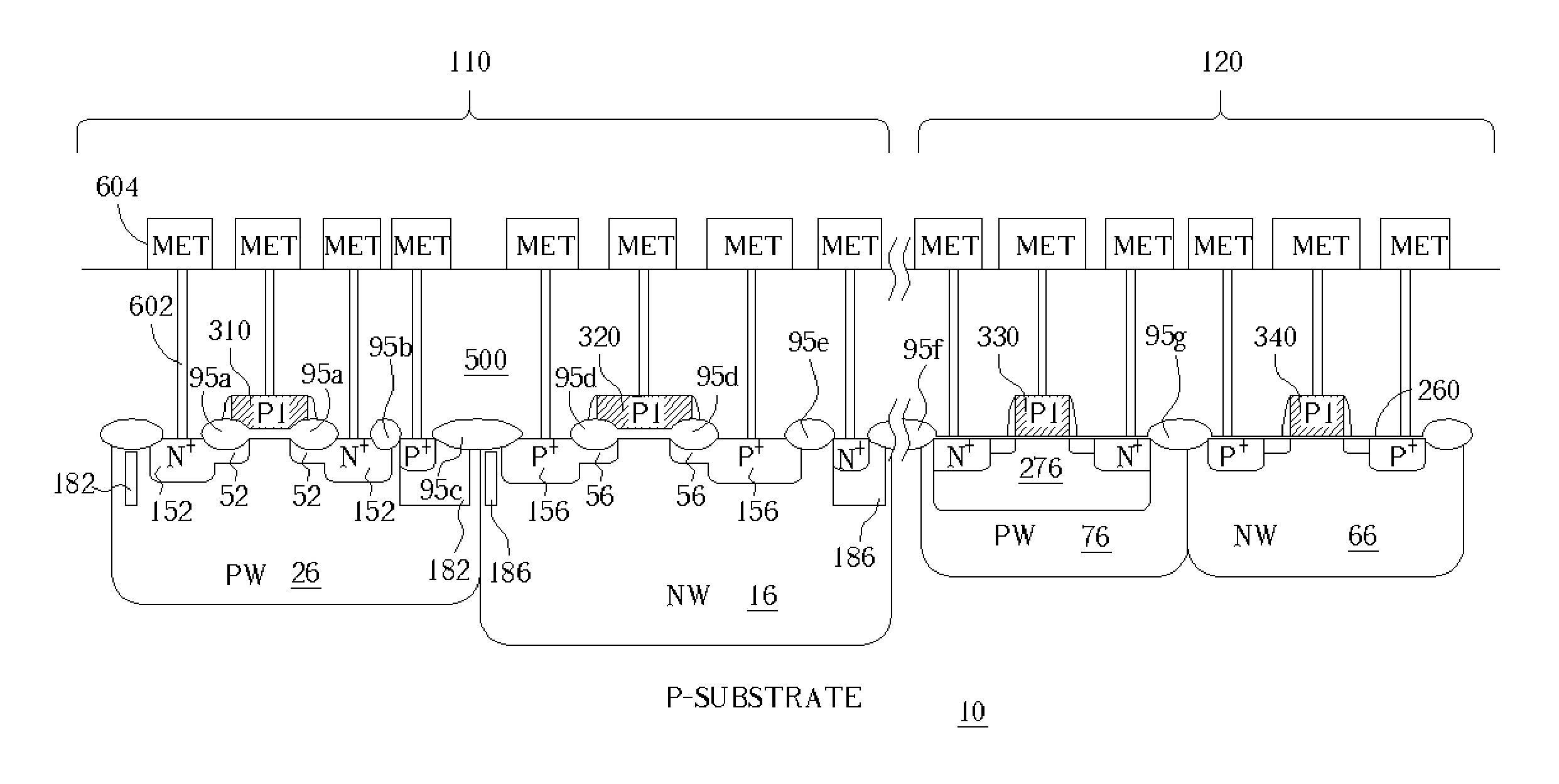
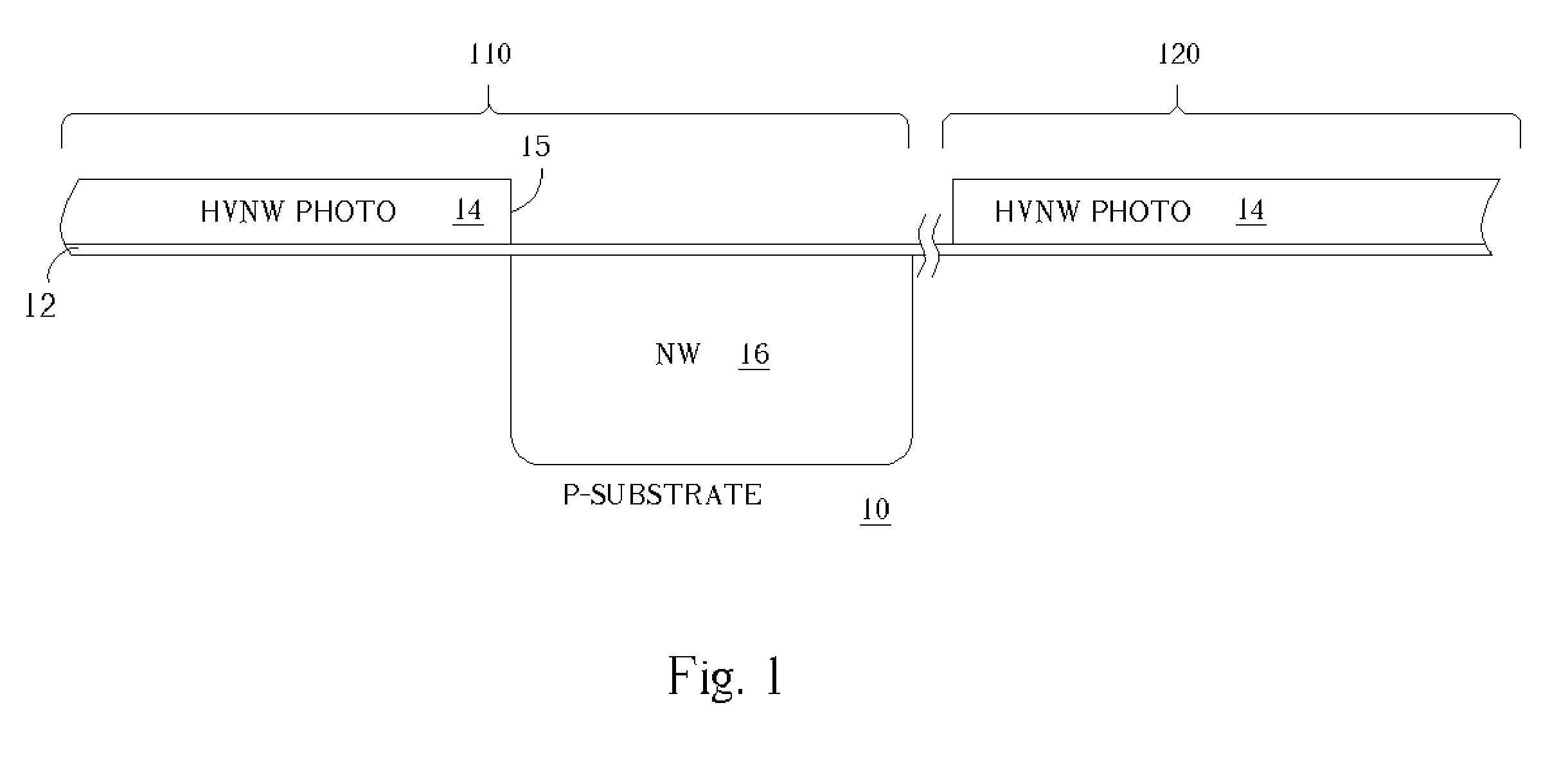
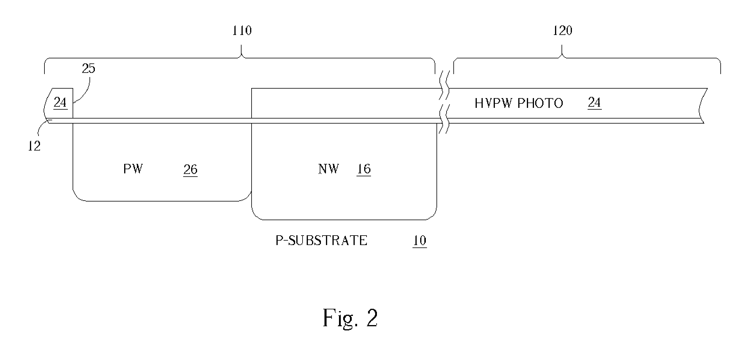
[0036] The present invention is directed to an improved method for making an integrated circuit having both high-voltage and low-voltage devices. It is noteworthy that the present invention is suited for making high-voltage MOS devices that have gate and drain terminals operated at a high voltage of about 30˜40V and low-voltage MOS devices that have gate and drain terminals operated at a relatively low voltage of about 3˜4V that is lower than conventional art (5˜6V). The gate oxide for the high-voltage MOS devices (also referred to as “high-voltage gate oxide”) has a thickness of about 700˜900 angstroms and the gate oxide for the low-voltage MOS devices (also referred to as “low-voltage gate oxide”) has a thickness of about 50˜70 angstroms. The present invention method is specifically suited for the manufacture of high voltage device having field oxide under gate structure and drift layers under the field oxide. The low-voltage devices according to this invention are particular LDD ...


PUM


Abstract

A high-voltage semiconductor MOS process that is fully compatible with low-voltage MOS process is provided. The high-voltage N/P well are implanted into the substrate prior to the definition of active areas. The channel stop doping regions are formed after the formation of field oxide layers, thus avoiding lateral diffusion of the channel stop doping regions. In addition, the grade drive-in process used to activate the grade doping regions in the high-voltage device area and the gate oxide growth of the high-voltage devices are performed simultaneously.

Description

BACKGROUND OF INVENTION [0001] 1. Field of the Invention [0002] The present invention relates generally to the manufacture of semiconductor MOS devices. More particularly, the present invention relates to a high-voltage semiconductor MOS making process that is compatible with low-voltage semiconductor MOS making process. [0003] 2. Description of the Prior Art [0004] Integrated circuits (ICs) containing both high-voltage and low-voltage devices such as high / low voltage MOS transistor devices are known in the art. For example, the low-voltage device may be used in the control circuits as the high-voltage device may be used in electrically programmable read only memory (EPROM) or the driving circuits of the liquid crystal display. [0005] Isolation structures such as field oxide layers, which increase the distance between the gate and the source / drain and further decrease the transverse electric field in the channel, are used for preventing short channel effects of the high-voltage MOS ...

Claims


Application Information

Patent Timeline
Patent Type & Authority Applications(United States)
IPC IPC(8): H01L29/78H01L21/8238
CPCH01L21/2652H01L21/823814H01L21/823857H01L29/7833H01L21/823892H01L29/1083H01L21/823878
Inventor CHEN, JUNG-CHINGLIN, JY-HWANGYANG, SHENG-HSIUNGSU, JIM
Owner UNITED MICROELECTRONICS CORP
Why Eureka
Try Eureka