Liquid crystal display device, method for repairing liquid crystal display device, and method for driving liquid crystal display device

a liquid crystal display device and display device technology, applied in static indicating devices, non-linear optics, instruments, etc., can solve the problems of not yet solved, operational defects of thin film transistors, and tft liquid crystal display devices often have point defects, so as to reduce the aperture ratio and suppress the effect of the operation defect rate and the reduction of the fabrication cos

Active Publication Date: 2006-01-26
SHARP KK
View PDF16 Cites 19 Cited by
  • Summary
  • Abstract
  • Description
  • Claims
  • Application Information

AI Technical Summary

Benefits of technology

[0032] According to the present invention, a defective pixel caused by an operational defect of a thin film transistor can be repaired to be a perfectly norm

Problems solved by technology

The TFT liquid crystal display device often has point defects due to operational defects of the thin film transistors which are the driving element.
Causes for the operational defects of the thin film transistors are various, e.g., formation defects of the channel unit, the inter-layer short, the intra-layer short between the source and the drain, etc. and are problems which have not yet been solved.
The TFT liquid crystal display device has a large number of pixels arranged in a matrix, and it is very difficult to perfectly prevent the generation of such defects.
Allowing defects of a part of the pixels to make the device as a whole effective lowers the product yield and resultantly increases the fabrication costs.
However, in the above-described first method for repairing the liquid crystal display device, although a dark point is less conspicuous than a luminous point, it cannot be said that such state is normal.
When pixel electrodes adjacent to each other along the extension of the drain bus line are interconnected, the pixels are for th

Method used


Image

  • Liquid crystal display device, method for repairing liquid crystal display device, and method for driving liquid crystal display device
  • Liquid crystal display device, method for repairing liquid crystal display device, and method for driving liquid crystal display device
  • Liquid crystal display device, method for repairing liquid crystal display device, and method for driving liquid crystal display device

Examples


first embodiment

A First Embodiment

[0047] The liquid crystal display device, the method for repairing the liquid crystal display device, and a method for driving the liquid crystal display device according to a first embodiment of the present invention, will be explained with reference to FIGS. 1 to 12.

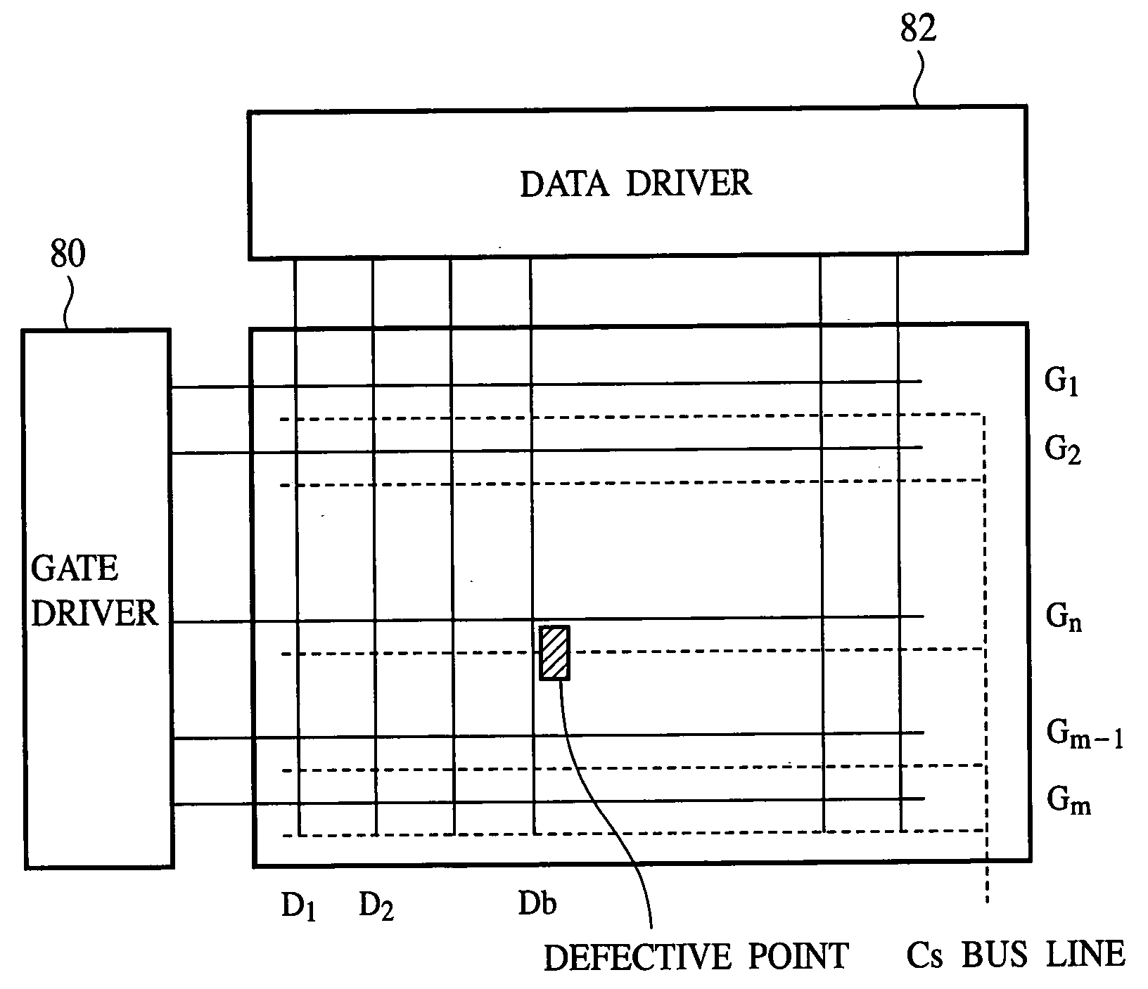
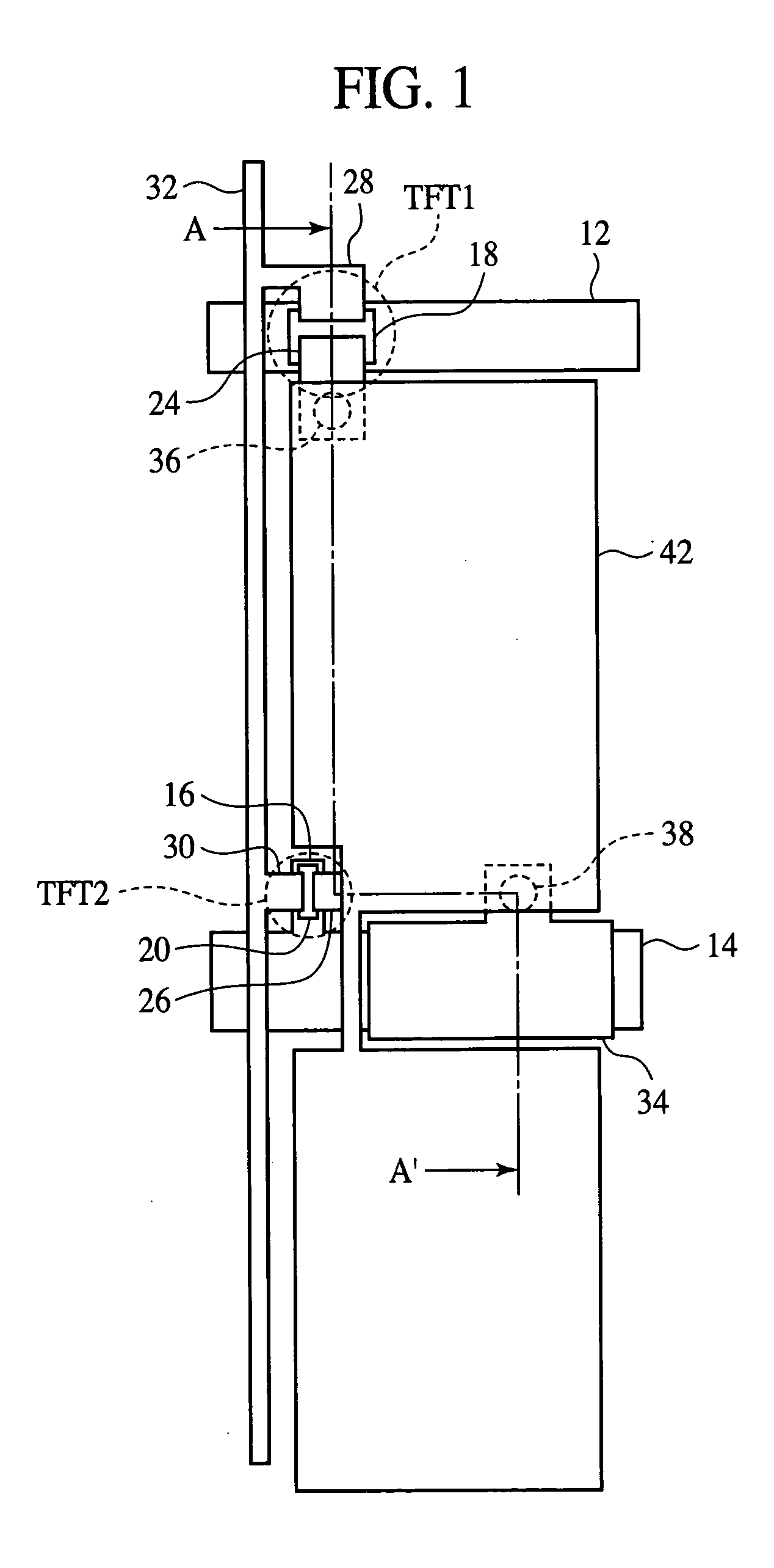
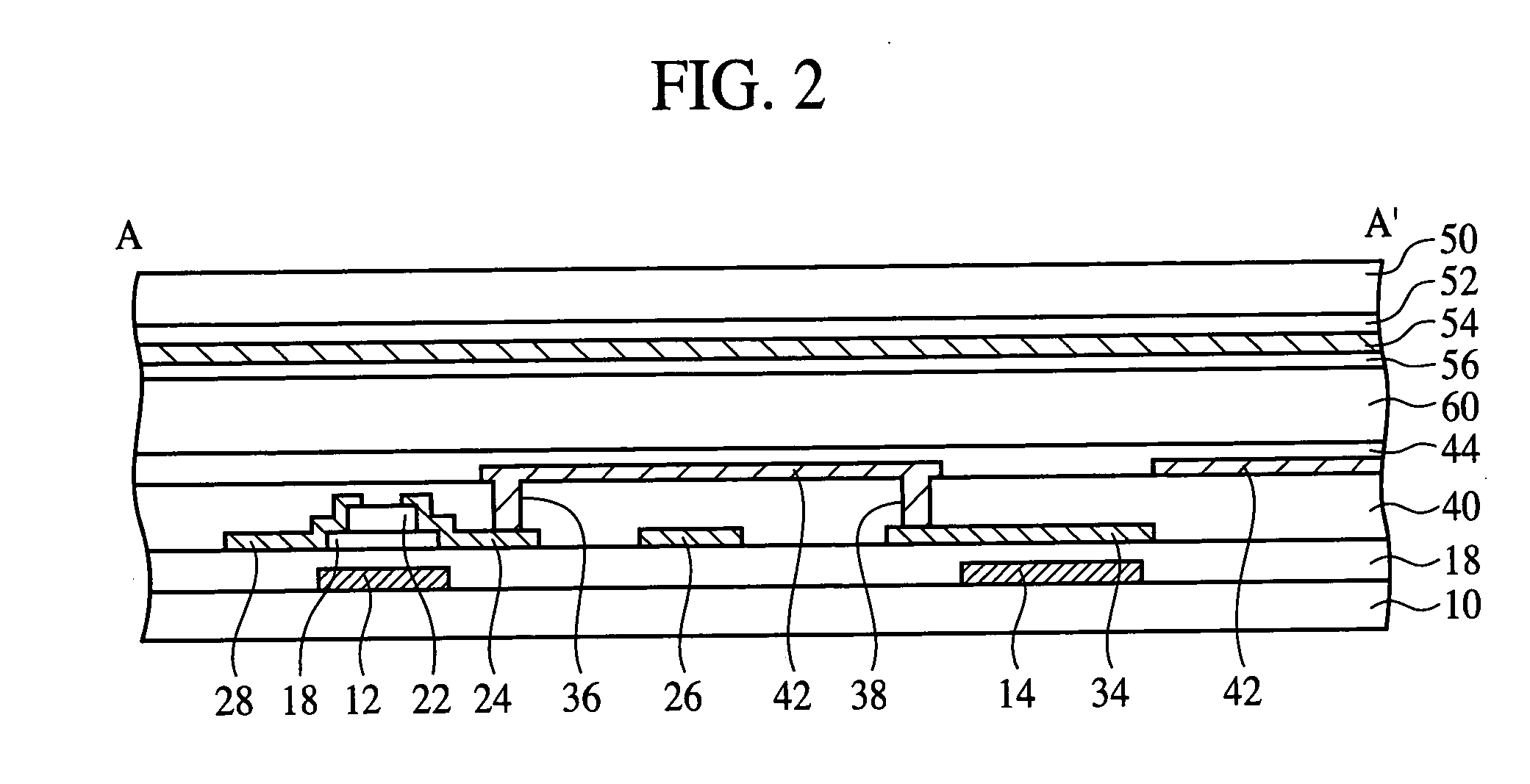
[0048]FIG. 1 is a plan view of the liquid crystal display device according to the present embodiment, which shows a structure thereof. FIG. 2 is a diagrammatic sectional view of the liquid crystal display device according to the present embodiment, which shows the structure thereof. FIG. 3 is a circuit diagram of the liquid crystal display device before repaired according to the present embodiment. FIG. 4 is a plan view of the liquid crystal display device after repaired according to the present embodiment, which shows the structure thereof. FIG. 5 is a circuit diagram of the liquid crystal display device after repaired according to the present embodiment. FIG. 6 is a plan view of the liquid crystal ...

second embodiment

A Second Embodiment

[0096] The liquid crystal display device, the method for repairing the liquid crystal display device, and the method for driving the liquid crystal display device according to a second embodiment of the present invention will be explained with reference to FIGS. 13 to 17. The same members of the present embodiment as those of the liquid crystal display device according to the first embodiment shown in FIGS. 1 to 12 are represented by the same reference numbers not to repeat or to simplify their explanation.

[0097]FIG. 13 is a plan view of the liquid crystal display device according to the present embodiment, which shows a structure thereof. FIG. 14 is a circuit diagram of the liquid crystal display device before repaired according to the present embodiment. FIG. 15 is a plan view of the liquid crystal display device after repaired according to the present embodiment, which shows a structure thereof. FIG. 16 is a circuit diagram of the liquid crystal display device...


PUM


Abstract

The liquid crystal display device comprises: a plurality of pixels arranged in a matrix, adjacent to each other row-wise and column-wise; a plurality of first bus lines extended row-wise and connected to the pixels arranged row-wise; a plurality of second bus lines extended column-wise and connected to the pixels arranged column-wise; and a plurality of third bus lines extended row-wise, connected to the pixels arranged row-wise, and being capable of applying a voltage which independently changes with time. Said plurality of the pixels each includes: a pixel electrode; a first switching element connected to the pixel electrode and the second bus line, for controlling the connection between the pixel electrode and the second bus line by the first bus line; and a second switching element having one electrode connected to the second bus line and the other electrode arranged, overlapping the pixel electrode with an insulating film formed therebetween, for controlling the connection between said one electrode and said the other electrode by the third bus line.

Description

CROSS-REFERENCE TO RELATED APPLICATIONS [0001] This application is based upon and claims the benefit of priority from the prior Japanese Patent Application No. 2004-211701, filed on Jul. 20, 2004, the entire contents of which are incorporated herein by reference. BACKGROUND OF THE INVENTION [0002] The present invention relates to a liquid crystal display device, more specifically, a liquid crystal display device which allows a defective pixel to be repaired to be normal, a method for repairing the liquid crystal display device, and a method for driving the display device. [0003] A liquid crystal display device makes image displays by applying electric fields partially a liquid crystal layer sandwiched between glass substrates to change an alignment direction of the liquid crystal to thereby change optical property of the liquid crystal. Recently, TFT liquid crystal display devices, which control the voltage to be applied to the pixel electrodes arranged in a matrix by thin film tran...

Claims


Application Information

Patent Timeline
IPC IPC(8): G09G3/36
CPCG02F1/13624G02F1/136259G02F1/136286G02F2001/136268G09G2330/10G09G3/3648G09G2300/0809G09G2320/0285G09G2330/08G02F2001/136272G02F1/136268G02F1/136272
Inventor KAMADA, TSUYOSHI
Owner SHARP KK
Why Eureka
Try Eureka