Semiconductor chip-embedded substrate and method of manufacturing same

Active Publication Date: 2006-02-02
SHINKO ELECTRIC IND CO LTD
View PDF33 Cites 32 Cited by
  • Summary
  • Abstract
  • Description
  • Claims
  • Application Information

AI Technical Summary

Benefits of technology

[0020] According to the present invention, by using semiconductor chips which have been stacked in advance, it is possible to provide a thin or miniature semiconductor chip-embedded substrate having semiconductor chips embedded therein in high density. The stack of semiconductor chips can be free from a lowering of positioning accuracy due to differences in coefficient of expansion, and can improve the precision of the semiconductor chip-embedded substrate and, accordingly, thereby enhan

Problems solved by technology

In any event, however, no attempt has been made to embed chips into a su

Method used


Image

  • Semiconductor chip-embedded substrate and method of manufacturing same
  • Semiconductor chip-embedded substrate and method of manufacturing same
  • Semiconductor chip-embedded substrate and method of manufacturing same

Examples


Embodiment Construction

[0025] Various embodiments of the present invention will be described below with reference to the drawings. It is to be understood that the present invention is by no means limited to these embodiments.

[0026] A stack of semiconductor chips is utilized in the semiconductor chip-embedded substrate of the present invention.

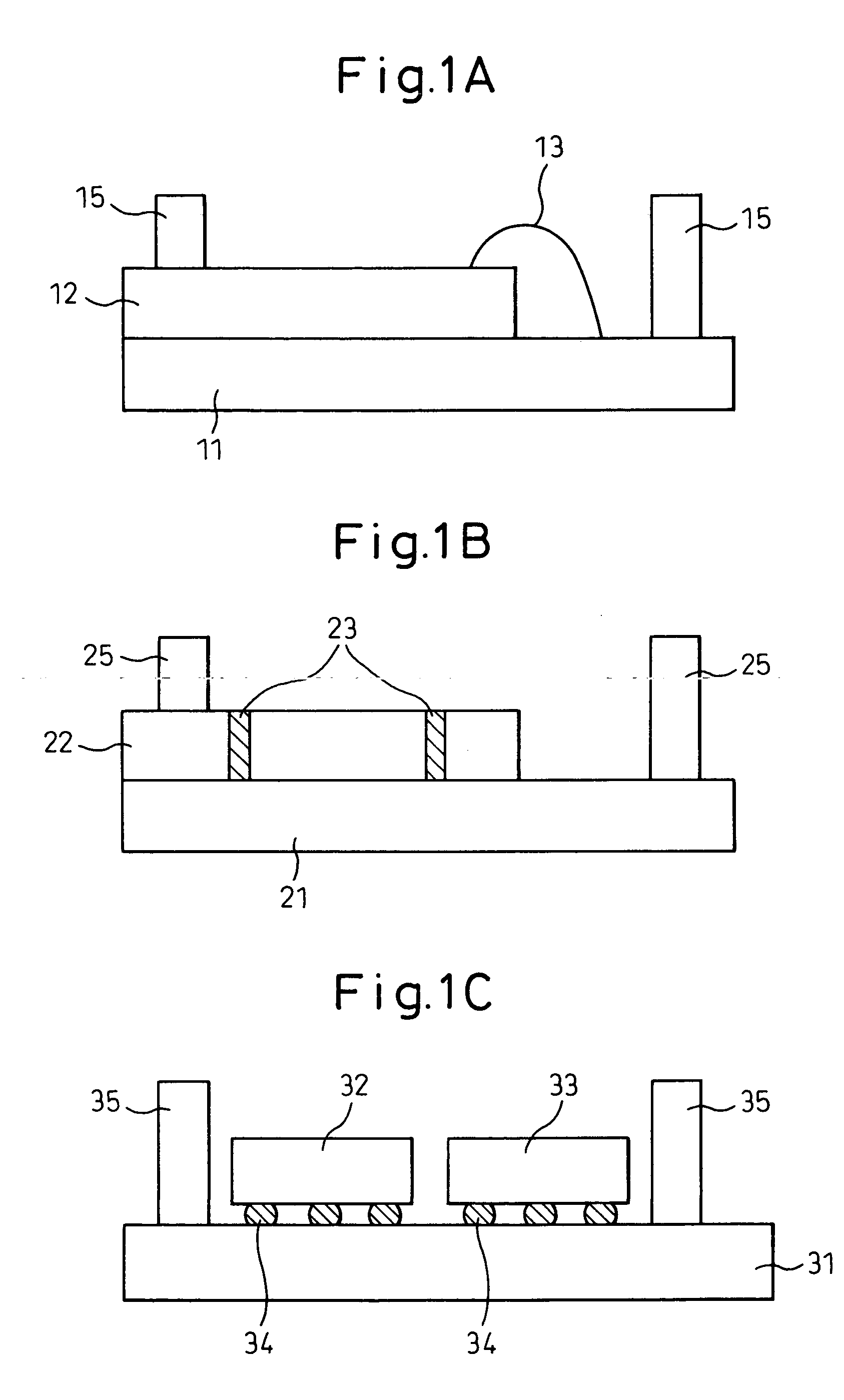
[0027]FIGS. 1A to 1C show examples of stacks of semiconductor chips conveniently used in the chip-embedded substrate of the present invention.

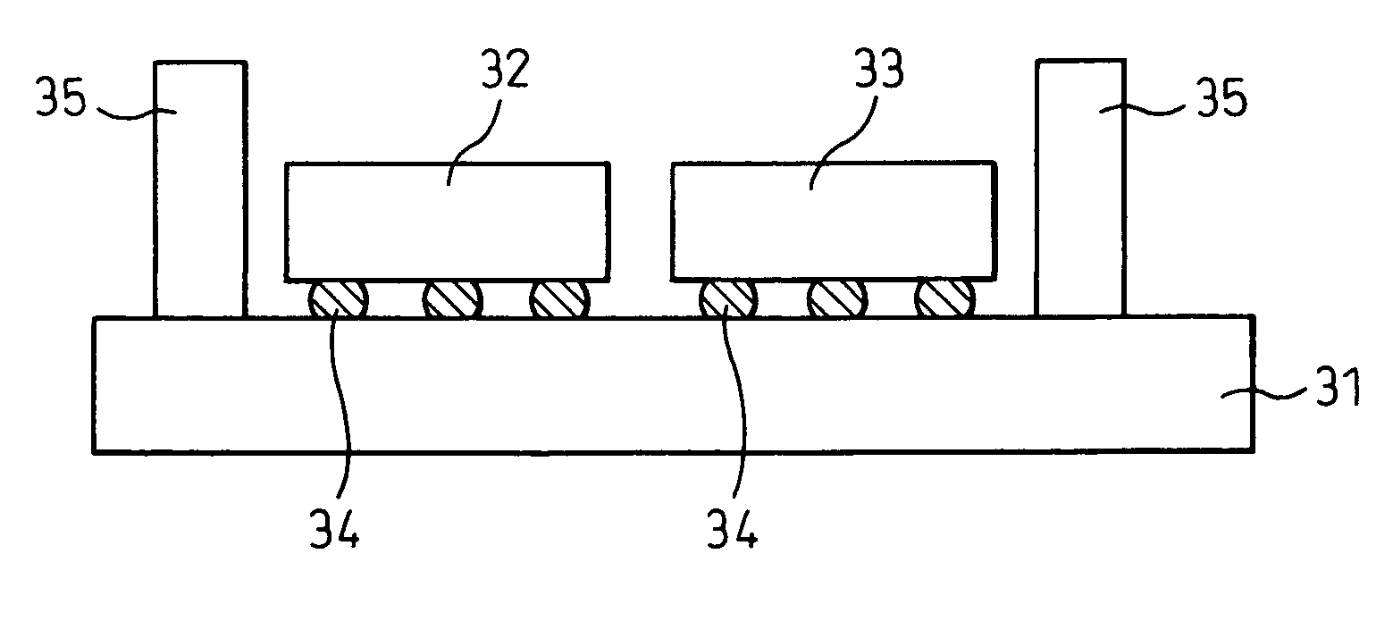
[0028] A stack shown in FIG. 1A is made by stacking two chips 11, 12 in a face-up fashion with electrical connection between the chips being done by wire bonding using wire 13. The connection between chips can be accomplished, for example, by a method in which a die attach tape (not shown) adhered to the rear surface of the upper chip 12 is used, and the chip 12 is disposed on the chip 11 to achieve connection of the two. On each of the chips 11, 12, a post 15 is formed for the connection to an external circuit. Another chip...


PUM


Abstract

A semiconductor chip-embedded substrate comprising a supporting substrate and an insulating layer thereon, members for the connection to external circuits, and a plurality of semiconductor chips embedded in the insulating layer, wherein at least some of the plurality of semiconductor chips are embedded as a stack or stacks thereof. A method of manufacturing such a semiconductor chip-embedded substrate is also disclosed.

Description

BACKGROUND OF THE INVENTION [0001] 1. Field of the Invention [0002] The present invention relates to a semiconductor chip-embedded substrate, and to a method of manufacturing same. [0003] 2. Description of Related Art [0004] Conventionally, in manufacturing a packaged substrate, for example, semiconductor chips are mounted on a substrate. In mounting chips, a single chip may be mounted, or plural chips may be mounted to form a package. In any event, however, no attempt has been made to embed chips into a substrate. [0005] In recent years, as the performance of electronic apparatus using semiconductor devices such as semiconductor chips has become higher and more elaborate, it is increasingly required to improve the packaging density of semiconductor chips and to reduce the size and footprint of a substrate having semiconductor chips mounted thereon. In order to meet these requirements, various substrates having semiconductor chips embedded, so-called chip-embedded substrate or semic...

Claims


Application Information

Patent Timeline
IPC IPC(8): H01L23/34
CPCH01L23/49816H01L2924/15311H01L24/24H01L24/82H01L2224/16225H01L2224/24226H01L2224/48091H01L2224/48227H01L2924/01013H01L2924/01029H01L2924/01078H01L2924/01079H01L2924/14H01L2924/15331H05K1/185H01L23/5389H01L2224/92244H01L2224/73267H01L2224/32225H01L2224/12105H01L2924/3511H01L24/48H01L2924/01005H01L2924/01006H01L2924/01033H01L2924/014H01L2924/00014H01L2924/00H01L2924/00011H01L2224/0401H01L2224/45099H01L2224/45015H01L2924/207
Inventor KOYAMA, TETSUYAKOBAYASHI, TSUYOSHI
Owner SHINKO ELECTRIC IND CO LTD
Why Eureka
Try Eureka