Two stage boost converter topology

a converter and topology technology, applied in the field of dcdc converters, can solve the problems increased size and cost of high current and high voltage rated mosfets, and higher conduction losses of converters requiring rdson rated mosfets, so as to reduce the conduction and turn on losses of switches, reduce the cost of conversion, and reduce the effect of high step up ratio applications

Active Publication Date: 2006-02-09
ASTEC INT LTD
View PDF5 Cites 31 Cited by
  • Summary
  • Abstract
  • Description
  • Claims
  • Application Information

AI Technical Summary

Benefits of technology

[0013] An advantage of the present invention is that it enables the use of much lower voltage and Rdson MOSFET switches that are smaller and less costly, and reduces switch conduction and turn on losses.
[0014] Another advantage of the present invention is that it is suitable for use in high step up ratio applications.
[0015] These and other embodiments, features, aspects, and advantages of the invention will become better understood with regard to the following description, appended claims and accompanying drawings.

Problems solved by technology

Drawbacks of such conventional boost converter circuits include the creation of switch voltage and current stresses resulting in low efficiency power conversion.
A drawback of the use of high current and high voltage rated MOSFETs is increased size and cost.
Consequently, a drawback of converters requiring higher Rdson rated MOSFETS is higher conduction losses.
A drawback of converter 20 is that it is not suitable for high power or high boost ratio applications.
More specifically, in high power applications or high boost ratio applications, the switching current at MOSFET 14 becomes high and the added capacitor 22 must be able to handle the high current demands, making it more difficult to find a suitable capacitor for a particular application.

Method used


Image

  • Two stage boost converter topology
  • Two stage boost converter topology
  • Two stage boost converter topology

Examples


Embodiment Construction

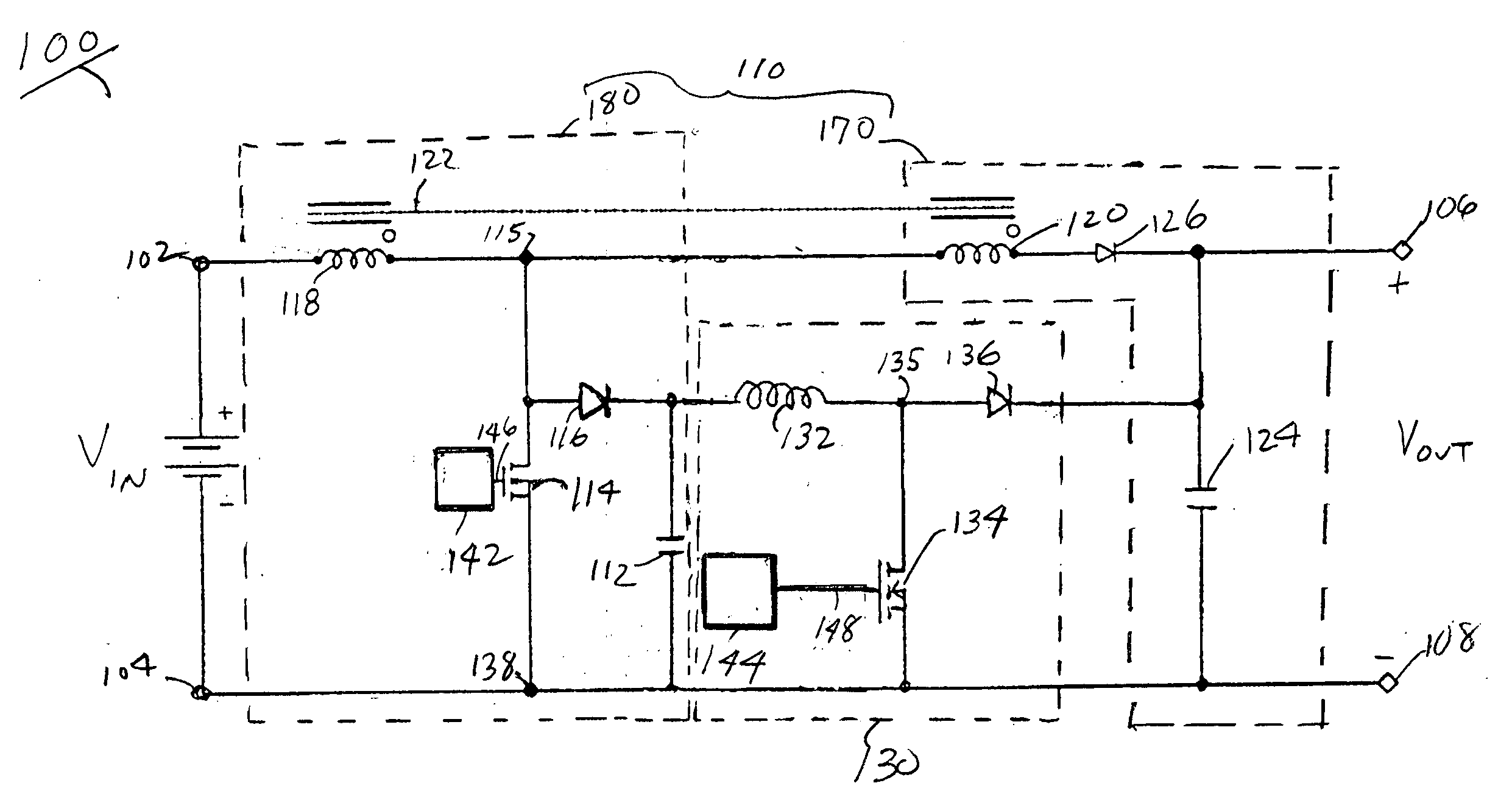
[0024]FIG. 3 is a schematic diagram of a preferred embodiment of the power converter 100 according to present invention. In a preferred embodiment, the power converter 100 has a boost converter topology including first 102 and second 104 input terminals where an input voltage is coupled and two output terminals 106, 108 where the output DC voltage is provided. Power converter 100 includes a two stage boost circuit 110 and a second boost converter 130. The two stage boost circuit 110 has a first stage circuit 180 and a second stage circuit 170. The two stage boost circuit 110 includes a magnetically coupled inductor 122 having a first winding 118 having one end connected to the first input terminal 102 and a second winding 120 connected to the other end of the first winding 118.

[0025] The first winding 118 of magnetically coupled inductor 122 is part of the first stage circuit 180. The first stage circuit 180 also includes a first switch 114 having a control input. The switch 114 is...


PUM


Abstract

A power converter having a two stage boost circuit and a small boost converter. The main power flow for the power converter is via the two stage booster circuit having a single switch. The voltage spike of the switch is clamped by a diode and a capacitor. The energy at the capacitor is transferred to the power converter's output terminals by the small boost converter. The two stage boost converter topology enables the use of much lower voltage and Rdson MOSFET switches so as to reduce cost, switch conduction loss and turn on loss.

Description

FIELD OF INVENTION [0001] The present invention relates in general to DC-DC converters, and more particularly, to a boost converter circuit topology for high power applications that utilizes a second smaller boost converter for reducing conduction loss and enabling the use of a substantially lower voltage rated MOSFET main boost switch. BACKGROUND OF INVENTION [0002] A boost converter is a power converter where a smaller input DC voltage is increased to a desired level. A prior art typical boost converter 10 is shown in FIG. 1. Boost converter 10 has input terminal 2, 4 for enabling an input voltage Vin to be coupled to converter 10, and output terminals 6, 8 where the output DC voltage is provided. The boost converter 10 includes an inductor 18, to which the input voltage Vin is coupled, that is in series with a boost diode 16 connected to an output capacitor 12 across which the load (not shown) is connected at terminals 6,8. A transistor switch 14 is connected to a node 15 between...

Claims


Application Information

Patent Timeline
Patent Type & Authority Applications(United States)
IPC IPC(8): G05F1/613
CPCH02M2001/007H02M3/155H02M1/007
Inventor YAN, CHENG CHUNG
Owner ASTEC INT LTD
Why Eureka
Try Eureka