Semiconductor memory device having local sense amplifier with on/off control

a memory device and local sense technology, applied in the field of semiconductor memory devices, can solve the problems of increasing the difficulty of amplifiers to detect data with a minimum voltage difference and amplify the voltage of data, and achieve the effect of increasing the trcd parameter and improving the performance of the semiconductor memory devi

Inactive Publication Date: 2006-02-09
SAMSUNG ELECTRONICS CO LTD
View PDF11 Cites 25 Cited by
  • Summary
  • Abstract
  • Description
  • Claims
  • Application Information

AI Technical Summary

Benefits of technology

[0015] It is possible to increase the tRCD parameter by adding a sense amplifier capable of amplifying a voltage of data between the data sense amplifier 130 and a bit line sense amplifier (not shown), thereby improving a performance of the semiconductor memory device.
[0016] Further, when the added sense amplifier can be turned on if necessary, it is possible to reduce an amount of current required to use the added sense amplifier.

Problems solved by technology

Accordingly, it becomes more and more difficult for amplifiers to detect data with a minimum voltage difference and amplify voltages of the data.

Method used


Image

  • Semiconductor memory device having local sense amplifier with on/off control
  • Semiconductor memory device having local sense amplifier with on/off control
  • Semiconductor memory device having local sense amplifier with on/off control

Examples


Embodiment Construction

[0048] Hereinafter, exemplary embodiments of the present invention will be described in detail with reference to the accompanying drawings. Like reference numerals denote like elements in the drawings.

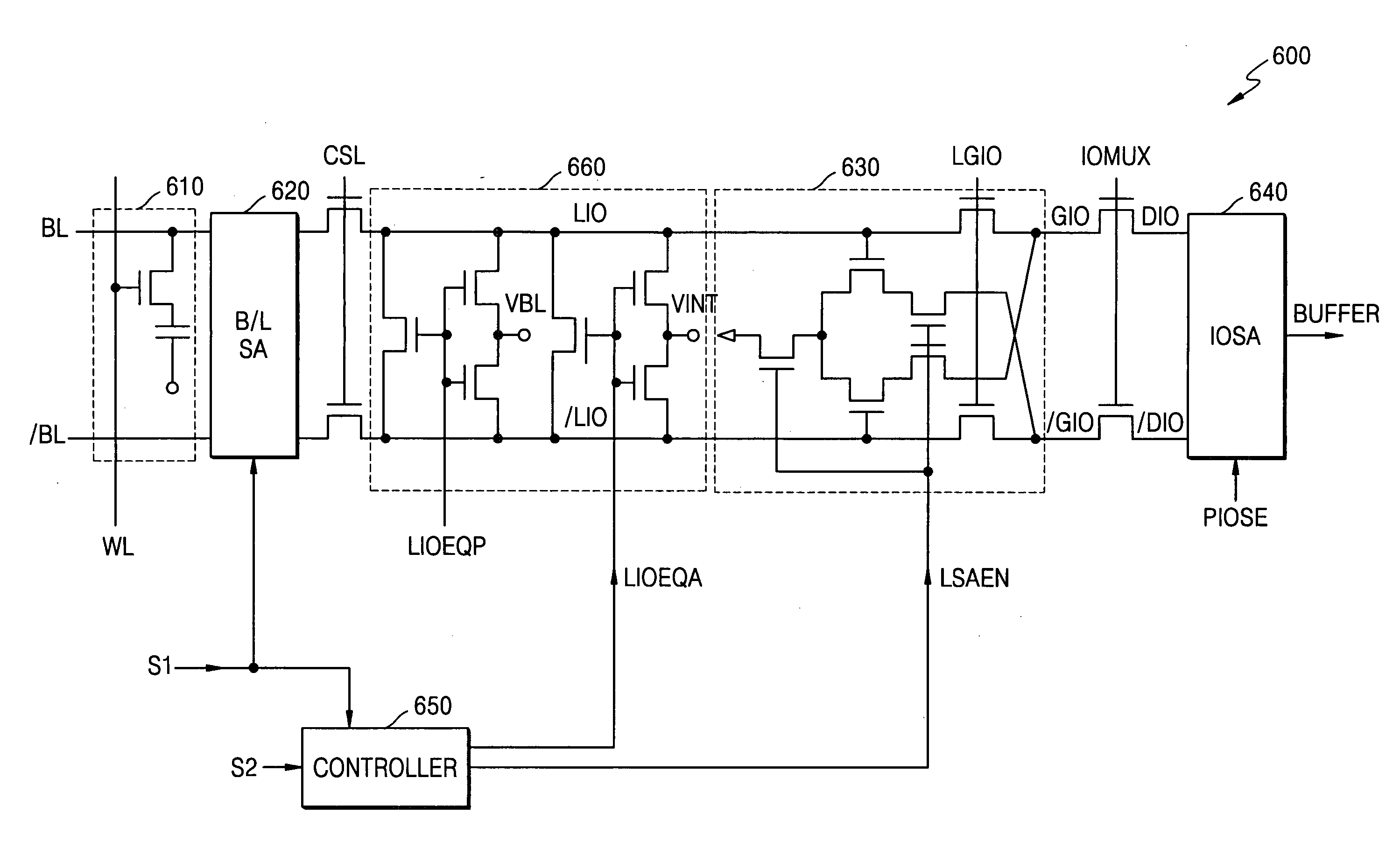
[0049]FIG. 3 is a circuit diagram of a semiconductor memory device 300 according to an embodiment of the present invention. FIG. 4 is a timing diagram of a read operation of the semiconductor memory device 300 according to an embodiment of the present invention.

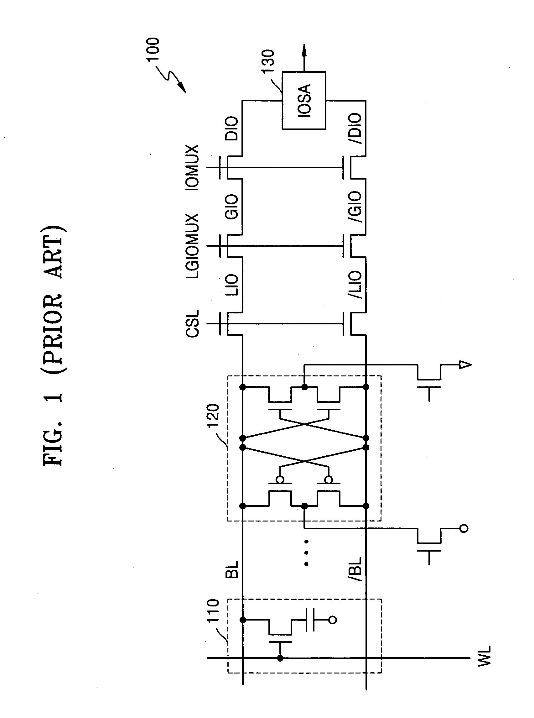
[0050] Referring to FIGS. 3 and 4, the semiconductor memory device 300 includes a plurality of memory cells 310 in an array block, a pair of local input / output (I / O) lines LIO and / LIO, a pair of global I / O lines GIO and / GIO, a local sense amplifier 320, a local I / O line precharge controller 360, and a data sense amplifier 330. The local sense amplifier 320 amplifies voltages of data output from the local I / O lines LIO and / LIO and then transmits the data to the global I / O lines GIO and / GIO, in response to a local sense cont...


PUM


Abstract

A semiconductor memory device includes a plurality of memory cell array blocks, a bit line sense amplifier, a local sense amplifier that can be controlled to be turned on or off, a data sense amplifier, and a controller. The controller activates a local sense control signal for a predetermined duration in response to first and second signals. The first signal is a bit line sense enable signal that activates the bit line sense amplifier, and the local sense amplifier is activated for a predetermined duration after the bit line sense enable signal is activated. The second signal is activated or deactivated in phase with a column selection line signal that connects a pair of bit lines and a pair of local input / output lines. Accordingly, it is possible to turn on or off the local sense amplifier according to operating conditions, thereby increasing a tRCD parameter and reducing the consumption of current. The operating speed of the semiconductor memory device can be improved by combining the local sense amplifier with a current type data sense amplifier that does not require precharging and equalization during a read operation.

Description

CROSS-REFERENCE TO RELATED PATENT APPLICATIONS [0001] This application claims the priority of Korean Patent Application No. 10-2004-0061090, filed on Aug. 3, 2004, in the Korean Intellectual Property Office, the disclosure of which is incorporated herein in its entirety by reference. BACKGROUND OF THE INVENTION [0002] 1. Field of the Invention [0003] The present invention relates to a semiconductor memory device, and more particularly, to a semiconductor memory device with a local sense amplifier that can be turned on only if required. [0004] 2. Description of the Related Art [0005] In a semiconductor memory device such as a dynamic random access memory (DRAM) or a synchronous random access memory (SRAM), data read in a read operation sequentially passes through a plurality of sense amplifiers and is then output. Since data read from a memory cell has a low voltage, the voltage of the data is amplified by a bit line sense amplifier. The amplified voltage of the data is amplified aga...

Claims


Application Information

Patent Timeline
Patent Type & Authority Applications(United States)
IPC IPC(8): G11C7/00
CPCG11C7/06G11C2207/065G11C2207/005G11C11/4091G11C7/08G11C7/12G11C11/4094G11C2207/063
Inventor SHIN, SANG-WOONGKIM, CHUL-SOOJUN, YOUNG-HYUNLEE, SANG-BO
Owner SAMSUNG ELECTRONICS CO LTD
Why Eureka
Try Eureka