EUV magnetic contrast lithography mask and manufacture thereof

a magnetic contrast and lithography technology, applied in the field of semiconductor fabrication, can solve the problems of local deposition of absorber-bearing gas, circuit to be improperly written, and the number of functioning chips per wafer is rastically reduced, and achieves high inspection contrast

Active Publication Date: 2006-02-09
INFINEON TECH AG
View PDF12 Cites 43 Cited by
  • Summary
  • Abstract
  • Description
  • Claims
  • Application Information

AI Technical Summary

Benefits of technology

[0030] An advantage of preferred embodiments of the present invention is that mask inspection requirements are decoupled from those of other steps in the mask manufacturing process. Mask materials generally do not require high EUV or optical contrast to conform to inspection requirements. Mask inspection will therefore generally not impose a requirement that is incompatible other layer requirements imposed by other process steps such as mask etch or repair.
[0031] A further advantage of a preferred embodiment of the present invention is that it may simultaneously meet the requirements for individual layers, specifically for the buffer layer, with respect to aspect ratio, patterning, compatibility with repair techniques and high inspection contrast.

Problems solved by technology

EUV masks have to be free of defects and particles since those would inevitably be imaged onto the wafer well, and will, in most cases, drastically reduce the number of functioning chips per wafer.
Mask defects will cause the circuit to be improperly written and, thus, malfunction.
Although Silicon has a large CTE that may result in undesirable displacement of printed images, Silicon also has a high thermal conductivity and thus may be a viable substrate as long as heat can be removed efficiently from the mask during exposure.
A focused ion beam can also cause local deposition from an absorber-bearing gas at a clear spot defect (dark field repair).
The requirements with respect to the individual layers in the process steps shown in FIGS. 2a-2h are very difficult to meet simultaneously.
On the other hand, thin layers decrease the time needed for removing bright field defects.
Balancing these competing processing requirements is especially difficult for the buffer layer, especially for inspection.
The large expense associated with mask fabrication requires that a mask not be discarded for small defects.
Even more importantly, a defective mask often leads to defective devices.
For masks used in step and repeat operations, i.e. reticles, a single mask defect can ruin an entire wafer.
For next generation lithography, such as EUV lithography, inspection is more difficult.
A problem is that contrast between the EUV mask layers is often inadequate.
However, some of these methods still remain limited to inspection at the UV / DUV wavelengths.

Method used


Image

  • EUV magnetic contrast lithography mask and manufacture thereof
  • EUV magnetic contrast lithography mask and manufacture thereof
  • EUV magnetic contrast lithography mask and manufacture thereof

Examples


Embodiment Construction

[0050] The making and using of the presently preferred embodiments are discussed in detail below. It should be appreciated, however, that the present invention provides many applicable inventive concepts that can be embodied in a wide variety of specific contexts. The specific embodiments discussed are merely illustrative of specific ways to make and use the invention, and do not limit the scope of the invention.

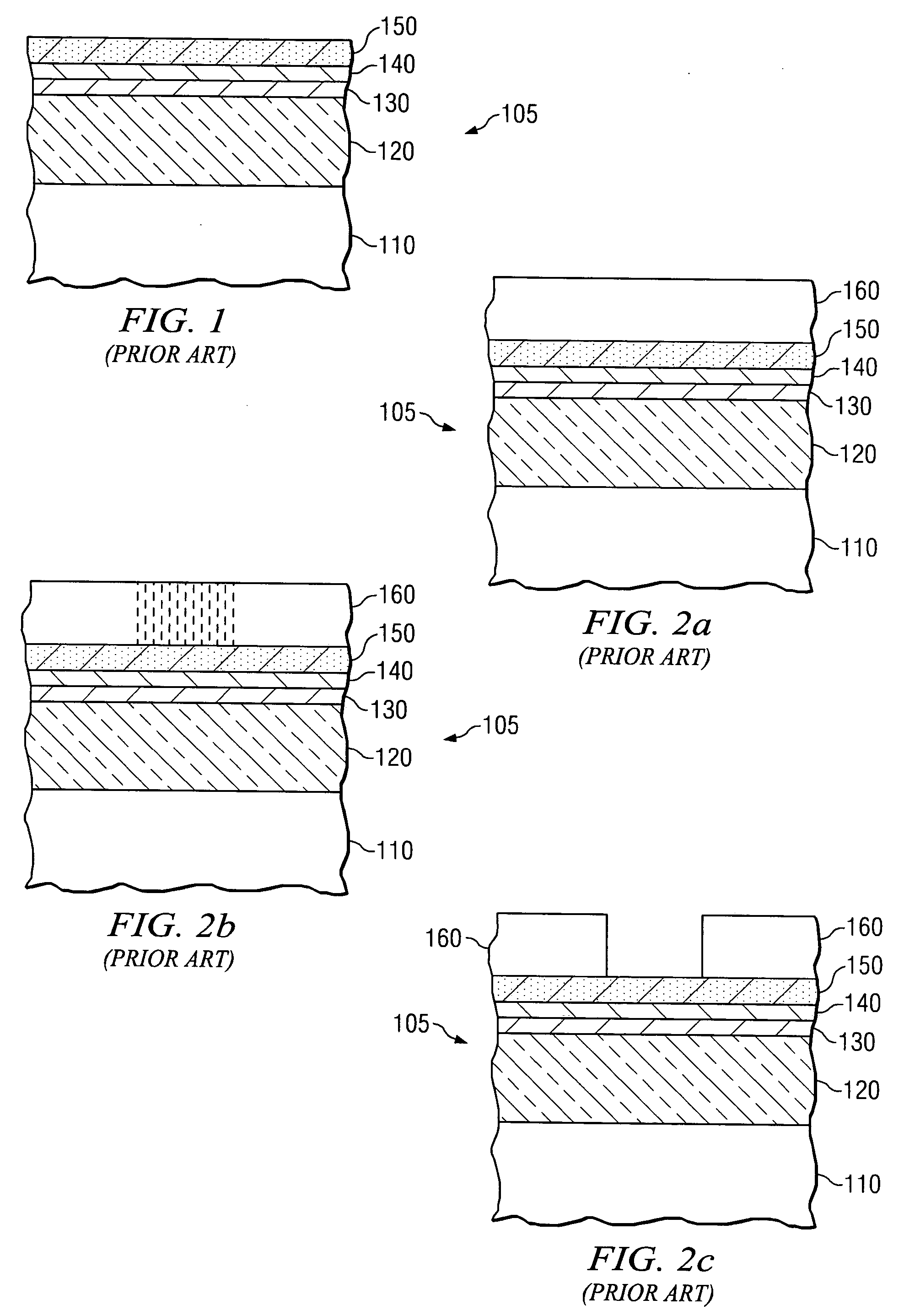
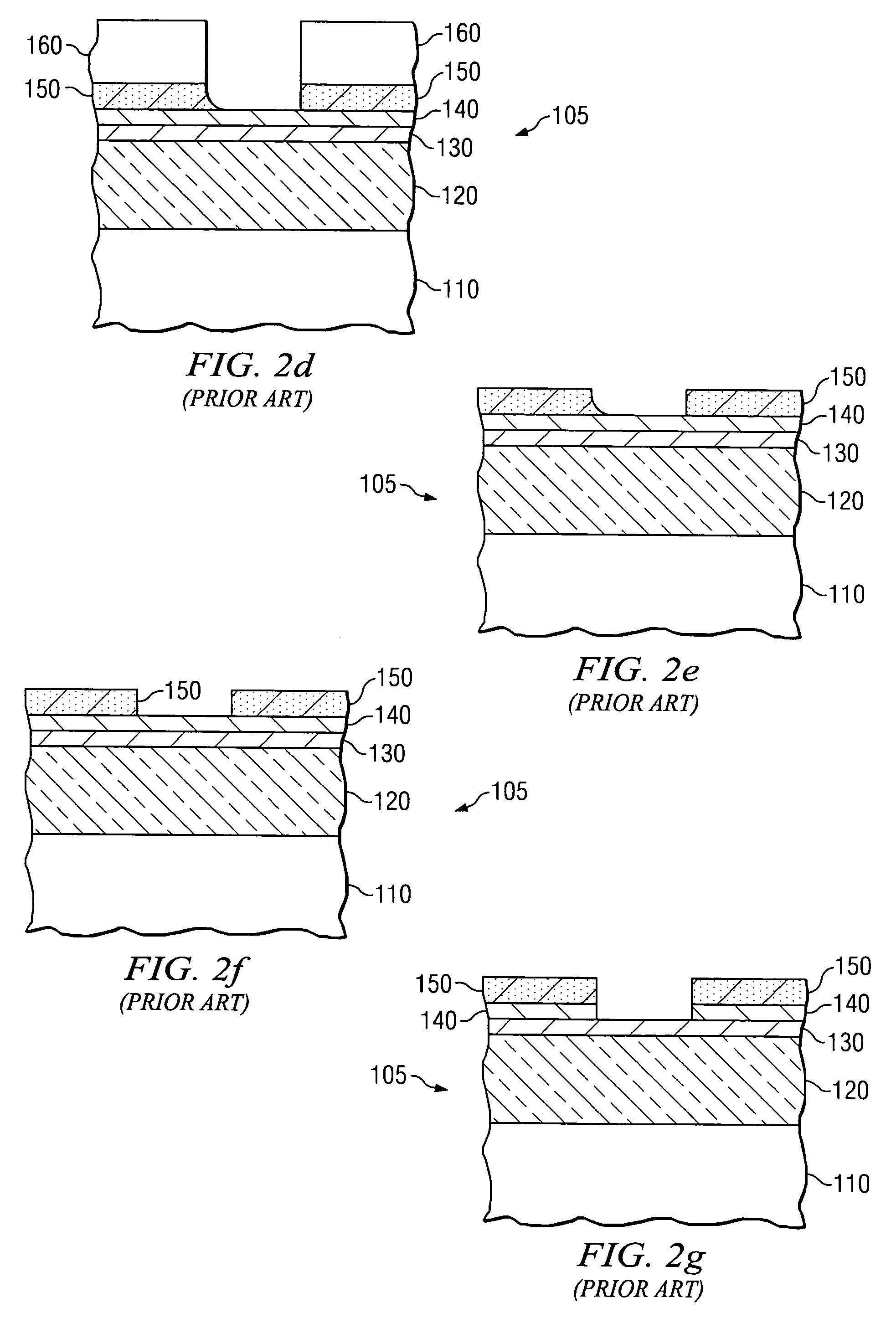
[0051] The present invention will be described with respect to preferred embodiments in a specific context, namely an EUV magnetic contrast mask. The invention may also be applied, however, to other next generation lithography methods such as X-ray or electron beam, for example.

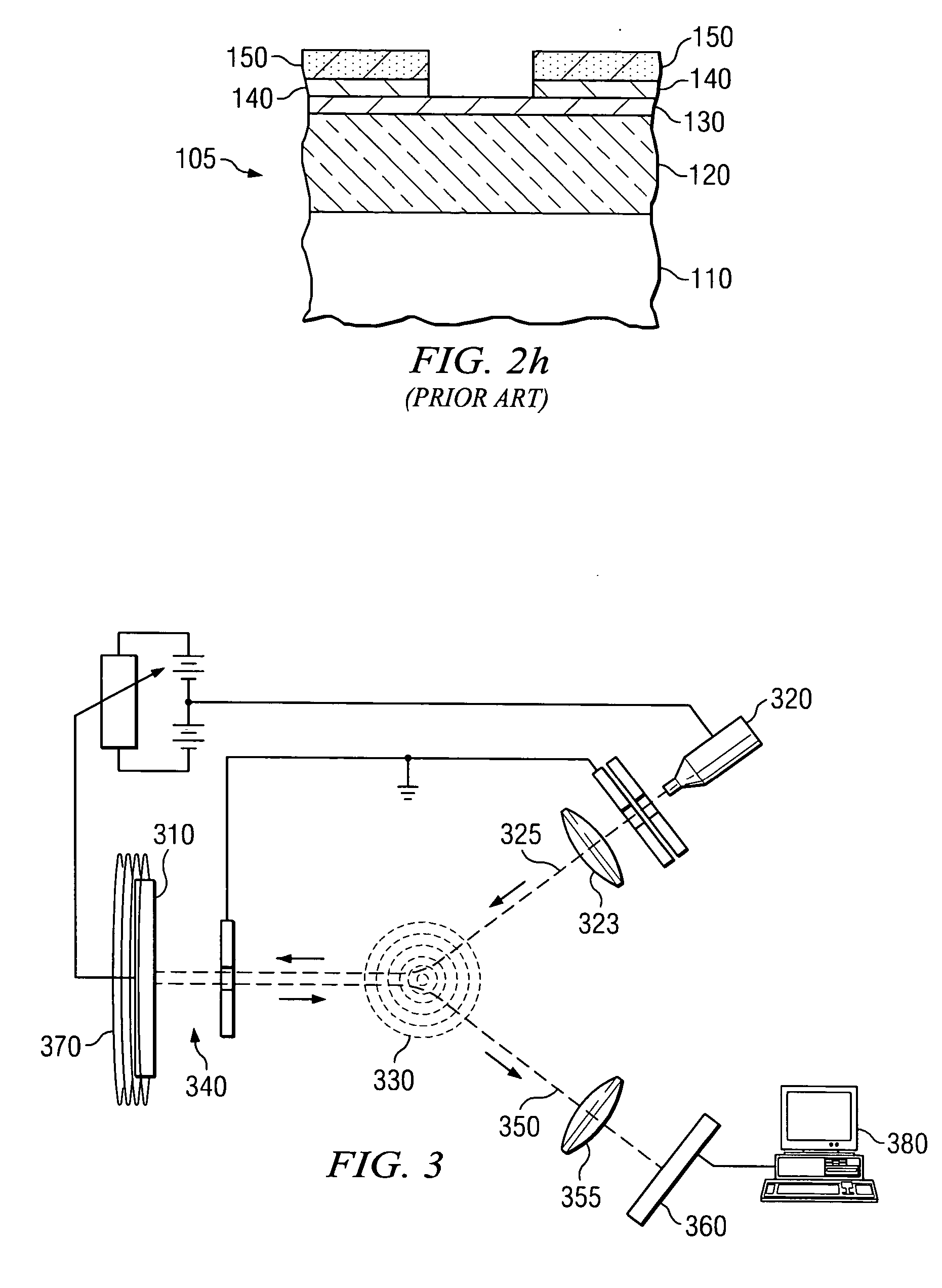
[0052] An Electron Mirror Microscope (EMM) is a preferred means for imaging and inspecting an EUV magnetic mask. Inspection after the absorber etch is preferred for it is at this point in mask fabrication that defects are best repaired or particles removed. In an EMM, the specimen is held at a high ...


PUM

PropertyMeasurementUnit
wavelengthsaaaaaaaaaa
atomic numberaaaaaaaaaa

Abstract

An EUV Lithography mask, a fabrication method, and use method thereof is provided. A preferred embodiment comprises a substrate, a Bragg reflector disposed upon the substrate, a buffer disposed upon the Bragg reflector, and an absorber layer disposed upon the buffer. The materials in the mask have selected magnetic properties. In a preferred embodiment, the buffer is a hard magnetic material, and the absorber is a soft magnetic material. Another preferred embodiment includes a mask manufacturing method further including a mask step. In a preferred embodiment, an electron mirror microscope is used to inspect the mask by imaging its topography with respect to its magnetic properties in an applied magnetic field.

Description

TECHNICAL FIELD [0001] The present invention relates generally to semiconductor fabrication, and more particularly to EUV lithography. BACKGROUND [0002] Lithography uses an imaging system that directs radiation onto a mask to form a pattern. It projects the image of that pattern onto a semiconductor wafer covered with light-sensitive photoresist. The pattern is formed from absorptive features or lines etched into the mask. The radiation used in lithography may be at any suitable wavelength, with the resolution of the system increasing with decreasing wavelength. The ability to print smaller features onto the semiconductor wafer improves as the resolution increases. [0003] Ongoing improvements in lithography have allowed the shrinkage of semiconductor integrated circuits (ICs) to produce devices with higher density and better performance. One highly promising lithography system uses radiation in the extreme ultraviolet (EUV) wavelength range. Generally, EUV radiation has wavelengths ...

Claims


Application Information

Patent Timeline
Patent Type & Authority Applications(United States)
IPC IPC(8): G01N21/00G06K9/00G21K5/00G03F1/00
CPCB82Y10/00G03F1/84G03F1/24B82Y40/00
Inventor SCHWARZL, SIEGFRIEDWURM, STEFAN
Owner INFINEON TECH AG
Why Eureka
Try Eureka