Method for manufacturing organic thin-film transistor with plastic substrate

a technology of organic thin film transistor and plastic substrate, which is applied in the manufacture of final products, basic electric elements, solid-state devices, etc., can solve the problems of plastic substrate, long fabrication time, and inability to use otft fabrication, and achieve the effect of reducing material cost and simplifying the fabrication procedur

Inactive Publication Date: 2006-02-09
IND TECH RES INST
View PDF3 Cites 16 Cited by
  • Summary
  • Abstract
  • Description
  • Claims
  • Application Information

AI Technical Summary

Benefits of technology

[0008] It is the primary object of the present invention to provide a method for manufacturing an organic thin-film transistor (OTFT) with a plastic substrate, characterized in that LIGA (Lithographie GalVanoformung Abformung) is used to define the electrode regions so that the fabrication procedure is simplified and the material cost is reduced.
[0009] It is another object of the present invention to provide a method for manufacturing an organic thin-film transistor with a plastic substrate, characterized in that conventional processes such as photo-lithography and etching are avoided so as to improve the yield and assure the device performance since undesirable etch may occur due to the chemicals utilized.
[0010] It is still another object of the present invention to provide a method for manufacturing an organic thin-film transistor with a plastic substrate, characterized in that the plastic substrate can separate the electrodes and enhance the carrier mobility due to lattice rearrangement of the organic semiconductor material such as pentacene.

Problems solved by technology

However, conventional manufacturing processes such as photo-lithography and etching may cause damages on the plastic substrate, and thus are not useful in OTFT fabrication.
Accordingly, there exist in conventional OTFT manufacturing processes some problems, such as: 1. longer fabrication time and higher material cost due to complicated processing steps; 2. lower yield due to undesirable substrate etch by chemicals during photo-lithography and etching processes; and 3. poorer electronic characteristics because the conventional glass substrate provides no alignment effect for the organic materials.

Method used


Image

  • Method for manufacturing organic thin-film transistor with plastic substrate
  • Method for manufacturing organic thin-film transistor with plastic substrate
  • Method for manufacturing organic thin-film transistor with plastic substrate

Examples


first embodiment

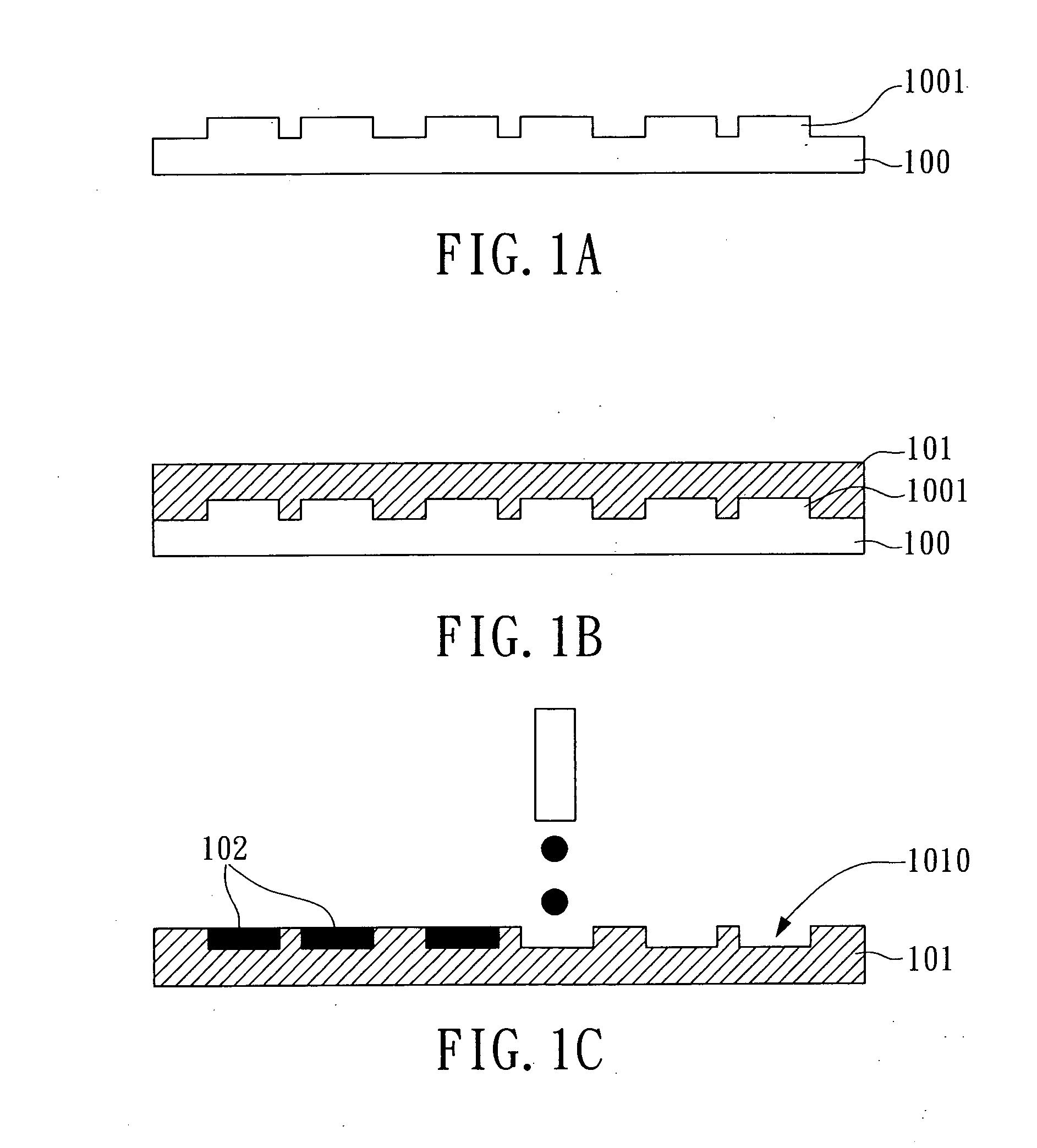
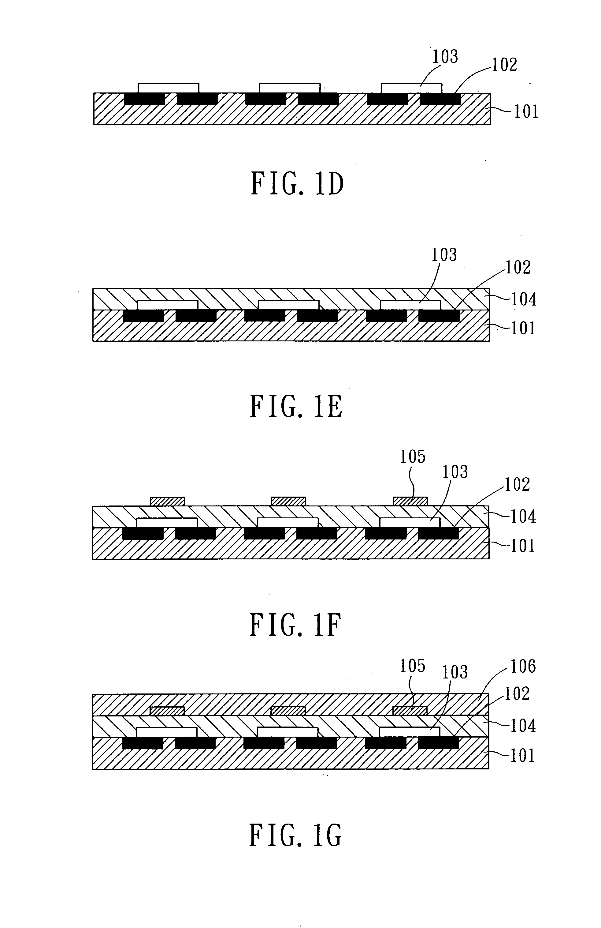
[0023] Please refer to FIG. 1A to FIG. 1G, which illustrate schematic diagrams showing steps in the method for manufacturing an organic thin-film transistor with a plastic substrate according to a first embodiment of the present invention. These steps are described hereinafter.

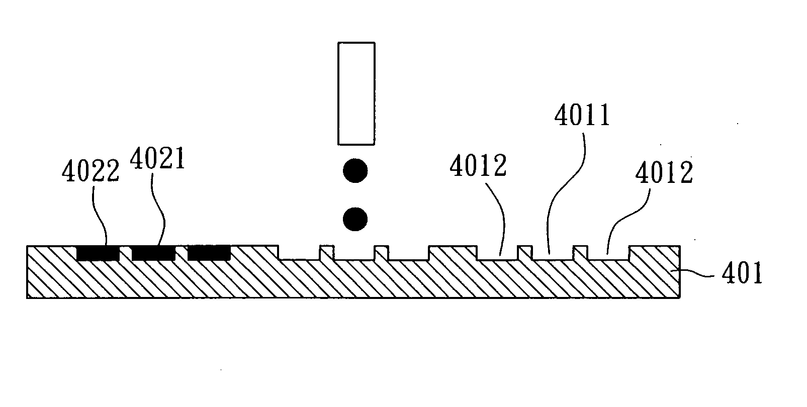
[0024] As shown in FIG. 1A, a mold 100 is provided with a relief printing structure 1001, which is implemented by LIGA (Lithographie GalVanoformung Abformung), resulting in higher aspect ratio and lower surface roughness. In LIGA process, the mold 100 is coated by a dry film or a polymer layer (not shown) of 10 μm˜1000 μm in thickness. Laser process is then performed on the dry film or the polymer layer so as to form the relief printing structure 1001.

[0025] As shown in FIG. 1B, the plastic substrate 101 is imprinted using the mold 100 so as to define the source / drain electrode regions 1010 as well as the channel length on the plastic substrate 101. In the first embodiment, the plastic substrate 101 comprise...

second embodiment

[0028] Please refer to FIG. 2A to FIG. 2G, which illustrate schematic diagrams showing steps in the method for manufacturing an organic thin-film transistor with a plastic substrate according to a second embodiment of the present invention. These steps are described hereinafter.

[0029] As shown in FIG. 2A, a mold 200 is provided with a relief printing structure 2001, which is implemented by LIGA (Lithographie GalVanoformung Abformung), resulting in higher aspect ratio and lower surface roughness.

[0030] As shown in FIG. 2B, the plastic substrate 201 is imprinted using the mold 200 so as to define the gate electrode regions 2010 on the plastic substrate 201. In the second embodiment, the plastic substrate 201 comprises polymer materials having —CH3 or —NH2 functional groups such as PMMA (poly-methylmethacrylate), mCOC (metallocenebased cyclic olefin copolymer), etc. The plastic substrate 201 is formed by imprinted without conventional photo-lithography and etching so as to reduce fab...

third embodiment

[0033] Please refer to FIG. 3A to FIG. 3G, which illustrate schematic diagrams showing steps in the method for manufacturing an organic thin-film transistor with a plastic substrate according to a third embodiment of the present invention. These steps are described hereinafter.

[0034] As shown in FIG. 3A, a mold 300 is provided with a relief printing structure 3001, which is implemented by LIGA (Lithographie GalVanoformung Abformung), resulting in higher aspect ratio and lower surface roughness.

[0035] As shown in FIG. 3B, the plastic substrate 301 is imprinted using the mold 300 so as to define the gate electrode regions 3010 on the plastic substrate 301. In the third embodiment, the plastic substrate 301 comprises polymer materials having —CH3 or —NH2 functional groups such as PMMA (poly-methylmethacrylate), mCOC (metallocenebased cyclic olefin copolymer), etc. The plastic substrate 301 is formed by imprinted without conventional photo-lithography and etching so as to reduce fabri...


PUM


Abstract

A method for manufacturing an organic thin-film transistor with a plastic substrate, comprising steps of: providing a mold and a plastic substrate, said mold being provided with a relief printing structure; imprinting said plastic substrate by said mold so as to define source / drain electrode regions on said plastic substrate; forming a first electrode layer so as to form source / drain electrodes on said source / drain electrode regions on said plastic substrate; forming a plurality of semiconductor mesas, each of said semiconductor mesas covering a pair of said source / drain electrodes; forming an insulating layer; forming a second electrode layer, being separated from and on said semiconductor mesas by said insulating layer; and forming a passivation layer.

Description

FIELD OF THE INVENTION [0001] The present invention generally relates to a method for manufacturing an organic thin-film transistor (OTFT) with a plastic substrate and, more particularly, to a method for forming an OTFT by imprinting as to define electrode regions. BACKFROUP OF THE INVENTION [0002] In recent years, organic thin-film transistors (OTFT's) have been widely used in various applications. More particularly, the OTFT is promising in flexible displays because it has advantages in lightness, thickness, portability, and flexibility. Plastic materials such as PMMA can change the alignment of organic materials such as pentacene. Therefore, PMMA is suitable for use as a substrate for OTFT. However, conventional manufacturing processes such as photo-lithography and etching may cause damages on the plastic substrate, and thus are not useful in OTFT fabrication. [0003] Accordingly, there exist in conventional OTFT manufacturing processes some problems, such as: [0004] 1. longer fab...

Claims


Application Information

Patent Timeline
Patent Type & Authority Applications(United States)
IPC IPC(8): H01L51/40H01L21/84
CPCH01L51/0005H01L51/0022H01L51/0097Y02E10/549H01L51/0545H01L51/105H01L51/0541Y02P70/50H10K71/135H10K71/611H10K77/111H10K10/466H10K10/464H10K10/84
Inventor HUANG, LIANG-YINGHO, JIA-CHONGLEE, CHENG-CHUNG
Owner IND TECH RES INST
Why Eureka
Try Eureka