Integrated circuit resistor

a technology of integrated circuit and resistor, which is applied in the direction of resistor details, semiconductor/solid-state device details, resistor details, etc., can solve the problems of reducing the overall size of the integrated device, limiting factors of resistors having relatively large resistance values, etc., and achieve accurate tuning of values and increase the resistance of resistance

Inactive Publication Date: 2006-02-16
RAYTHEON CO
View PDF8 Cites 0 Cited by
  • Summary
  • Abstract
  • Description
  • Claims
  • Application Information

AI Technical Summary

Benefits of technology

[0007] According to still another embodiment of the present invention, the removal of portions of the semiconductor layer to increase the resistance of the resistance between the first and second contact points is accomplished in at least two etching steps to creat

Problems solved by technology

For some applications, resistors having relatively large resistance values have become a limiting factor in the attempts to reduce the overall size of the integrated devices.
However, if a particular elec

Method used


Image

  • Integrated circuit resistor
  • Integrated circuit resistor
  • Integrated circuit resistor

Examples


Embodiment Construction

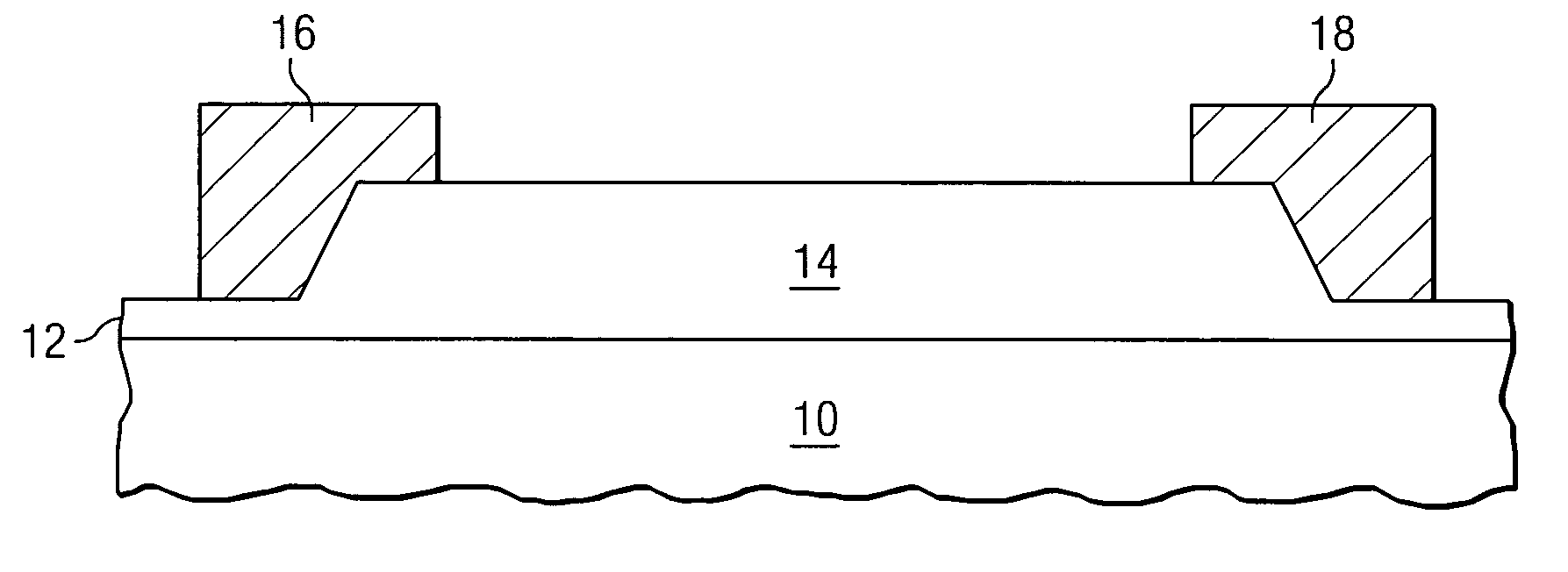
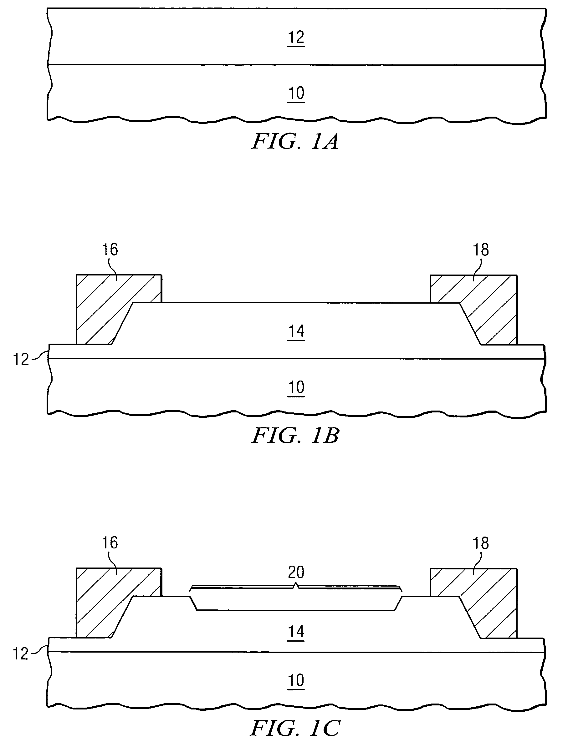
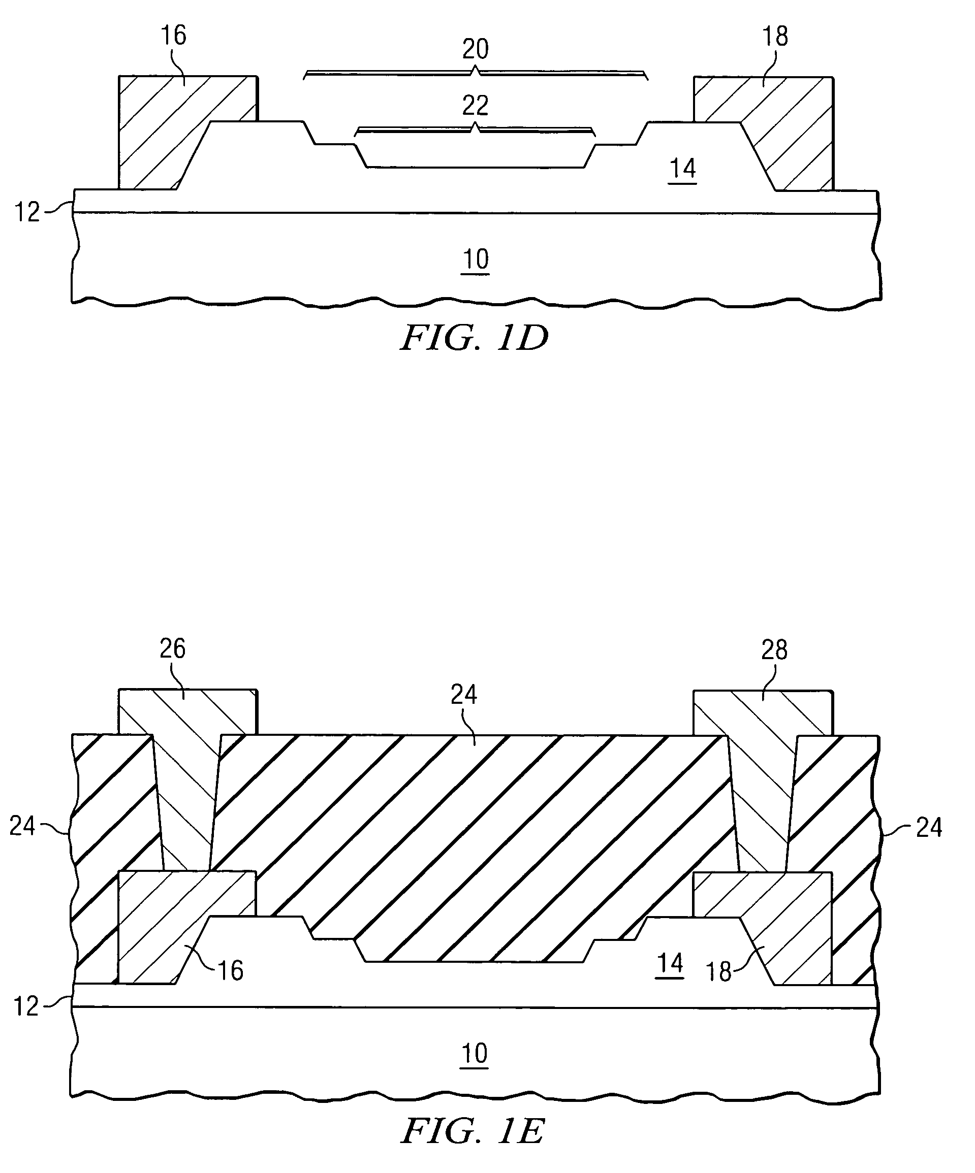
[0010] Referring to FIG. 1A, a semiconductor substrate 10 is illustrated. Substrate 10 may comprise silicon, germanium, gallium arsenide, silicon germanium, indium phosphide, gallium nitride, indium gallium phosphide, silicon carbide, or other suitable material. An epitaxial layer 12 of semiconductor material is formed using conventional epitaxial techniques on the outer surface of substrate 10. Epitaxial layer 12 may comprise any number of sequentially formed layers comprising different materials. As will be discussed herein, epitaxial layer 12 may comprise interstitial etch stop layers that may be used in later etching processes to provide etch depths that can be very accurately controlled. For example, one possible sequence of forming epitaxial layer 12 comprises the formation first of a super-lattice buffer layer comprising the alternating sequence of 15 Angstrom gallium arsenide layers with 200 Angstrom aluminum gallium arsenide layers. These alternating sequences can be done t...


PUM


Abstract

An integrated circuit resistor is provided that comprises a mesa 14 between electrical contacts 16 and 18. The electrical resistance between electrical contacts 16 and 18 is selectively increased through the formation of recesses 20 and 22 in the mesa 14. The size of recesses 20 and 22 can be used to tune the value of the electrical resistance between contacts 16 and 18.

Description

TECHNICAL FIELD OF THE INVENTION [0001] This invention relates in general to the field of electronic devices and more particularly, to an improved integrated circuit resistor and method for forming the same. BACKGROUND OF THE INVENTION [0002] In order to form the complex systems required to meet today's integrated electronics market, integrated circuits must contain a variety of active and passive elements all formed on a common substrate. For some applications, resistors having relatively large resistance values have become a limiting factor in the attempts to reduce the overall size of the integrated devices. [0003] Typical techniques to construct resistors and integrated circuits involve the deposition or growth of semiconductive films on the outer surfaces of the semiconductor substrate or outer layers. Contact points are then made to the films and the area of the film and the spacing of the contacts are used to adjust the resistance value of the resistor. These techniques can e...

Claims


Application Information

Patent Timeline
IPC IPC(8): H01L23/58
CPCH01L27/0802H01L27/0605H01L27/06
Inventor HESTON, DAVID D.MOONEY, JON E.
Owner RAYTHEON CO
Why Eureka
Try Eureka