Nitride semiconductor light emitting device

Active Publication Date: 2006-02-23
SHARP FUKUYAMA LASER CO LTD
View PDF7 Cites 18 Cited by
  • Summary
  • Abstract
  • Description
  • Claims
  • Application Information

AI Technical Summary

Benefits of technology

[0031] In the nitride semiconductor light emitting device, preferably, the width of the hill is 400 μm or more. As a result of this, the flatness on the surface of the nitride semiconductor growth layer that is layered on the hill can be made excellent.
[0032]

Problems solved by technology

In the conventional manufacture of a nitride semiconductor laser device which is a type of nitride semiconductor light emitting device, however, a problem arises where the yield, that is, the ratio of the number of devices obtained as good products to the total number of nitride semiconductor laser devices fabricated on one wafer is very low.
Such occurrence of cracking, in some cases, is caused by defects in the substrate.
So far, however, high quality GaN single crystal substrates that match the lattice of GaN have not yet been developed.
However, such SiC substrates are expensive, and it is difficult to increase the diameter thereof, and in addition, tensile strain may occur, and as a result, cracking easily occurs.
However, sapphire substrates do not

Method used


Image

  • Nitride semiconductor light emitting device
  • Nitride semiconductor light emitting device
  • Nitride semiconductor light emitting device

Examples


Embodiment Construction

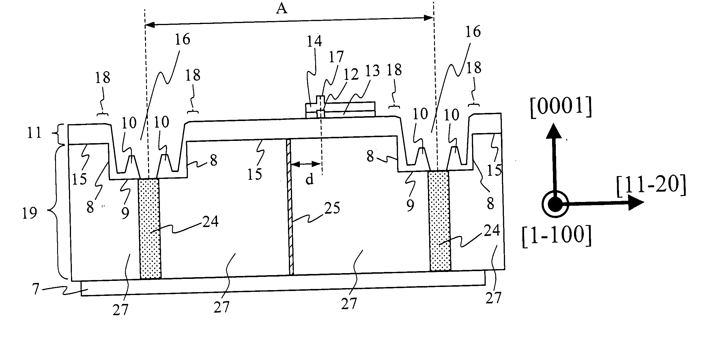
[0058] The definition of some terms is clarified in advance, in order to describe a variety of embodiments according to the present invention in the following. First, “dug out region” described in the present specification means a trench which is a recess that has been processed in stripe form in the surface of a processed substrate 19, for example, as shown in the below described FIG. 4b, and “hill” means a region that becomes a protrusion that has been processed in stripe form and a region excluding dug out regions.

[0059]“Nitride semiconductor substrate” described in the present specification means a substrate made of AlxGayInzN (0≦x≦1; 0≦y≦1; 0≦z≦1; x+y+z=1). Here, approximately 10% or less of the nitride elements within the nitride semiconductor substrate may be replaced other elements such as As, P or Sb (as long as the hexagonal system of the substrate is maintained). In addition, Si, O, Cl, S, C, Ge, Zn, Cd, Mg or Be may be doped into the nitride semiconductor substrate. Si,...


PUM


Abstract

A first region and a second region that has a defect density of which the value is higher than that of the first region are respectively formed so as to be aligned in stripe form in the direction parallel to the direction in which a dug out region extends, where atoms that terminate the surface of the first region are different from atoms that terminate the surface of the aforementioned second region, and the dug out region includes the first region and the second region.

Description

BACKGROUND OF THE INVENTION [0001] This application is based on Japanese Patent Application No. 2004-239467, filed on Aug. 19, 2004. FIELD OF THE INVENTION [0002] The present invention relates to a nitride semiconductor light emitting device such as a nitride semiconductor laser device. DESCRIPTION OF THE PRIOR ART [0003] Nitride semiconductors such as GaN, AlGaN, GaInN and AlGaInN have band gaps Eg which are greater than those of AlGaInAs-based semiconductors and AlGaInP-based semiconductors, and have features such that they are direct transition semiconductor materials. For this reason, these nitride semiconductors have attracted attention as materials for forming semiconductor light emitting devices, such as semiconductor lasers which can emit light having a short wavelength ranging from ultraviolet rays to green light, and light emitting diodes which cover a broad range of emitted light waves ranging from ultraviolet rays to red light, and are widely applicable to high density o...

Claims


Application Information

Patent Timeline
IPC IPC(8): H01L29/06
CPCB82Y20/00H01L33/007H01S5/34333H01S5/3202H01S5/0207H01S5/2201H01S2304/12H01S5/320275
Inventor TSUDA, YUHZOHKAMIKAWA, TAKESHI
Owner SHARP FUKUYAMA LASER CO LTD
Why Eureka
Try Eureka