

Processing method for flexible-rigid board of high-pixel camera module
A technology of soft-rigid combination board and camera module, which is applied in the direction of electrical components, simultaneous processing of multiple printed circuits, and printed circuit manufacturing, etc. It can solve problems that affect product yield and delivery time, long processing process, and damaged flatness. , to achieve the effect of reducing processing costs, good flatness, and saving plates
- Summary
- Abstract
- Description
- Claims
- Application Information
AI Technical Summary
Problems solved by technology
Method used
Image

Examples
Embodiment Construction
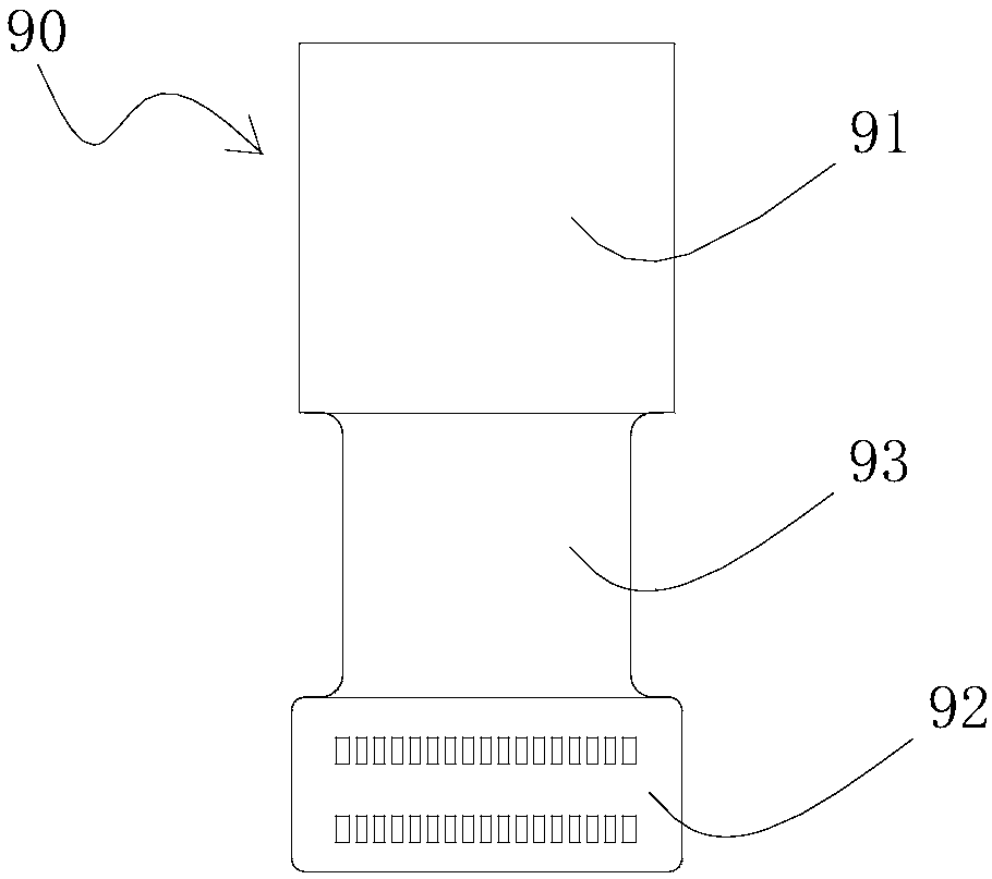
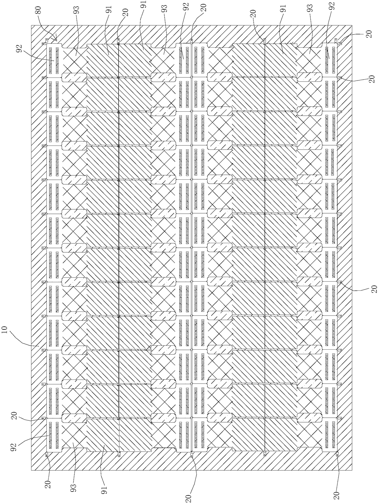
[0021] like Figure 2-4 As shown, a method for processing a rigid-flex board of a high-pixel camera module includes the following steps:
[0022] S1, according to the design requirements, etch out the circuit of several rigid-flex boards 90 arranged without gaps on the original board 10, and obtain the connecting board 80 ( That is, the high-pixel camera module is arranged in a combination of soft and hard boards), and at the same time, all the copper on the laser cutting path is etched away, so that the inner and outer layers of the laser cutting path are not covered with copper, saving cutting time. Improve cut quality.
[0023] In the embodiment, the distance between the inner circuit and the outer circuit of each rigid-flex board 90 and the outer edge of the rigid-flex board 90 is 0.2 mm to prevent the inner circuit from overlapping with the outer circuit. Misalignment, cutting the line during laser cutting, resulting in scrap.
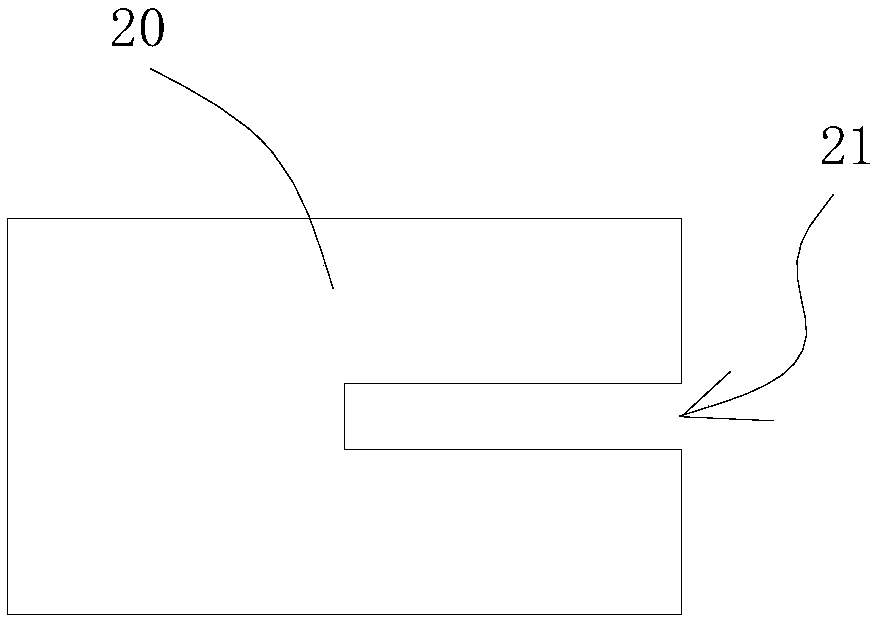
[0024] A laser cutting analyzer PAD 20 i...
PUM
 Abstract
Description
Claims
Application Information