Display device
a technology of a display device and a display screen, which is applied in the direction of discharge tubes/lamp details, discharge tubes/lamp details, cathode ray tubes/electron beam tubes, etc., can solve the problems of deterioration of the airtightness of the inside of the substra
- Summary
- Abstract
- Description
- Claims
- Application Information
AI Technical Summary
Benefits of technology
Problems solved by technology
Method used
Image

Examples
first embodiment
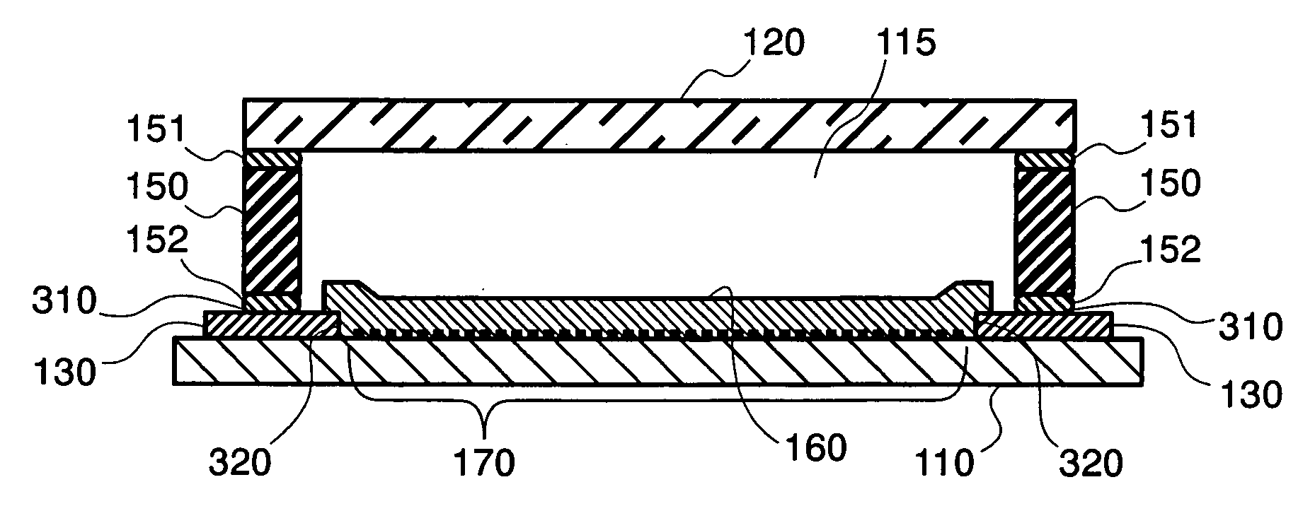
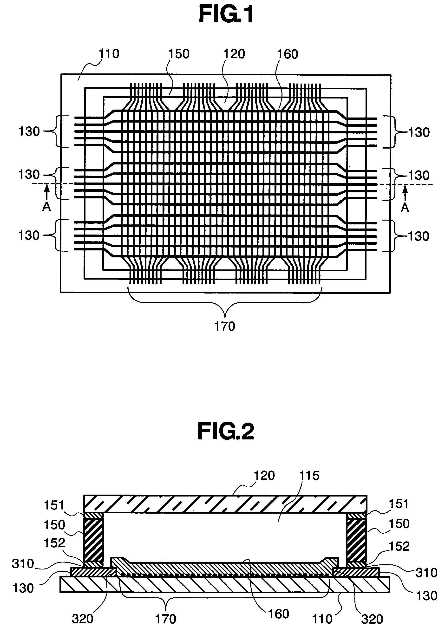
[0038]FIG. 1 is a plane view showing a schematic configuration of an FED (Field Emission Display) substrate according to a first embodiment of the invention. FIG. 2 is a section view along an A-A direction of the FED substrate of FIG. 1. As shown in the figures, the FED substrate of the embodiment is configured in a way that a cathode substrate 110 and an anode substrate 120 are disposed oppositely via frame glass 150.
[0039] The cathode substrate 110 is formed by an insulative substrate such as glass. Data lines 170 and scan lines 160 are provided crosswise on the cathode substrate 110. The data lines 170 are formed from Al or Al alloys. Thickness of the data lines 170 is typically within a range of 100 to 500 nm. Ends of the data lines 170 are connected to a data-line drive circuit (not shown) that is an external circuit.
[0040] Each of the scan lines 160 is typically formed from Ag, Au, Cu, and Pd or alloys of them, however, it is preferably formed from Ag in terms of low resista...
second embodiment
[0059]FIG. 6 is a plane view of an FED substrate according to a second embodiment. FIG. 7 is a section view along an A-A direction of FIG. 6. Description is omitted on parts that are configured in the same way as in the FED substrate of the first embodiment.
[0060] In the FED substrate of the first embodiment, the scan-line lead lines 130 were formed by wiring lines of Al in small thickness to secure the airtightness at the sealing portion 310. Moreover, the scan lines 160 were formed by wiring lines of Ag having low resistance to reduce resistance of the scan lines 160. On the contrary, in this embodiment, as shown in figures, the scan-line lead lines 130 extend to an area of scan lines, and forms part of scan lines 1302. To reduce resistance of the scan lines, wiring lines 1602 of Ag having low resistance is overlapped the scan line portion 1302. That is, the scan lines are formed by a combination of the wiring 1302 and the wiring 1602.
[0061] The scan-line lead lines 130 partiall...
third embodiment
[0071]FIG. 11 is a plane view of an FED substrate according to a third embodiment. FIG. 12 is a section view along an A-A direction of FIG. 11. Description is omitted on parts that are configured in the same way as in the FED substrate of the first and second embodiments.
[0072] In the FED substrate of the second embodiment, the scan-line lead lines 130 were extended to an area of scan lines, forming part of scan lines 1302. In addition, to reduce resistance of the scan lines, wiring lines 1602 of Ag having low resistance were overlapped on the scan line portion 1302. On the contrary, as shown in FIG. 11 and FIG. 12, the FED substrate of this embodiment has a configuration where, first, scan lines 1603 are formed on the data lines 170 by wiring lines of Ag having low resistance, and then wiring lines 1303 extending to the scan-line lead-line portion are overlapped them.
[0073] The scan lines 1603 are typically formed from Ag, Au, Cu, Pd or alloys of them, similarly as the scan lines...
PUM
 Abstract
Description
Claims
Application Information
 - R&D
- Intellectual Property
- Life Sciences
- Materials
- Tech Scout
- Unparalleled Data Quality
- Higher Quality Content
- 60% Fewer Hallucinations
Browse by: Latest US Patents, China's latest patents, Technical Efficacy Thesaurus, Application Domain, Technology Topic, Popular Technical Reports.
© 2025 PatSnap. All rights reserved.Legal|Privacy policy|Modern Slavery Act Transparency Statement|Sitemap|About US| Contact US: help@patsnap.com