Semiconductor device

a technology of semiconductor devices and diodes, applied in semiconductor devices, diodes, electrical apparatus, etc., can solve the problems of reducing the operating efficiency of the device, so as to achieve the effect of improving the operation

Active Publication Date: 2006-03-02
MITSUBISHI ELECTRIC CORP
View PDF5 Cites 14 Cited by
  • Summary
  • Abstract
  • Description
  • Claims
  • Application Information

AI Technical Summary

Benefits of technology

[0014] It is an object of the present invention is to provide a semiconductor device which

Problems solved by technology

The first conventional example given above has the disadvantage that a higher value of the resistance between the base and emitter of the PNP transistor results in a higher conducting resistance during reverse conduction and thus inhibits the reverse conducting capability.
On the other hand, a lower value of the resistance, during turn-on of the IGBT, disadvantageously causes both electrons from the emitter side of the IGBT and holes from the collector side of the IGBT to flow into the resistance without flowing into the base of the PNP transistor.
This mak

Method used


Image

  • Semiconductor device
  • Semiconductor device
  • Semiconductor device

Examples


first preferred embodiment

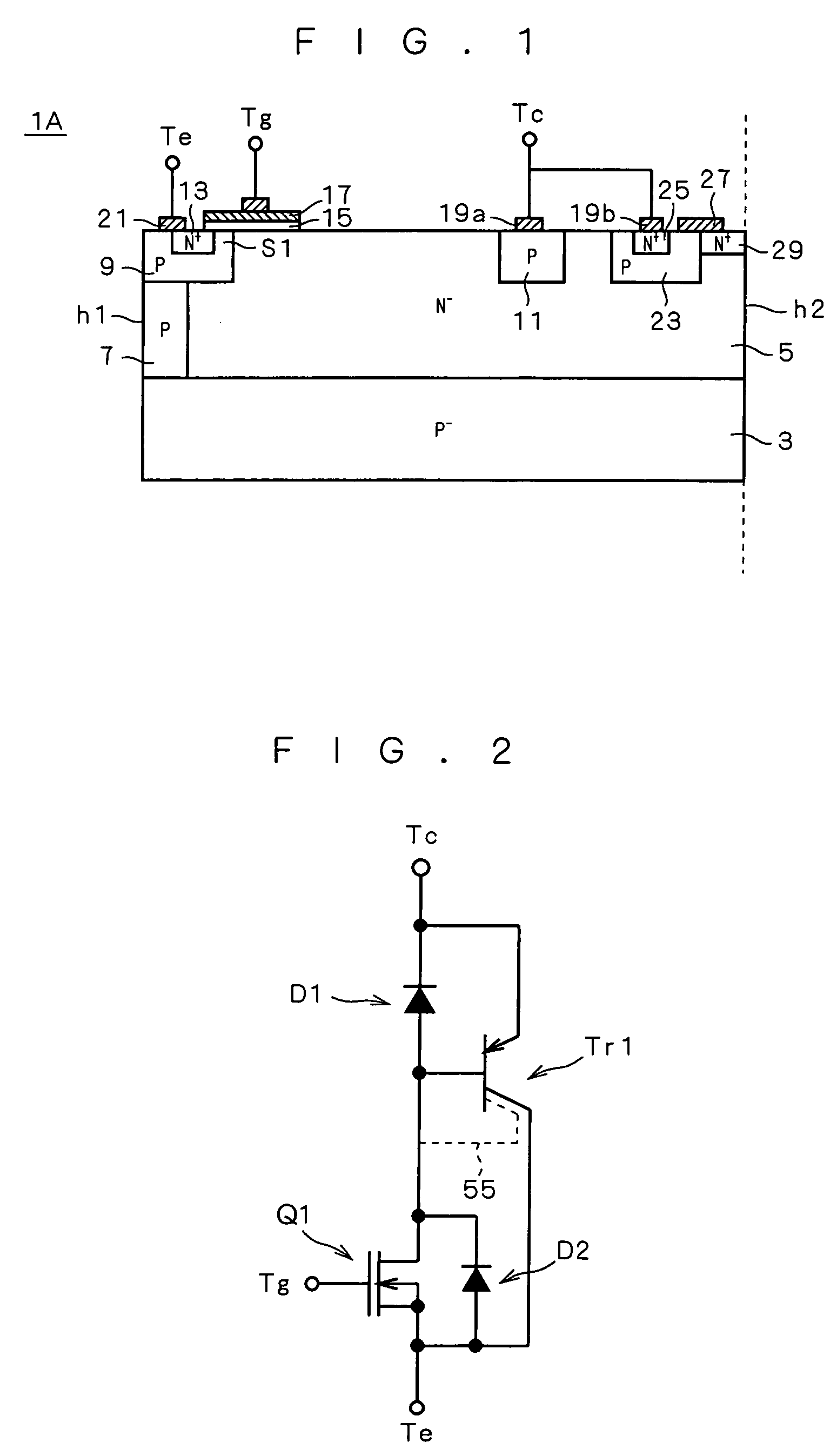
[0032] A semiconductor device 1A according to this preferred embodiment is a lateral collector-shorted IGBT. It includes, as shown in FIG. 1, a P− substrate 3 (semiconductor substrate of a first conductivity type); an N− epitaxial layer 5 (semiconductor layer of a second conductivity type) formed on one main surface of the P+ substrate 3; a P diffusion region 9 (first semiconductor region of the first conductivity type) formed in the surface of the N− epitaxial layer 5 and connected to the P+ substrate 3 through a P diffusion region 7 (semiconductor region of the first conductivity type); a P diffusion region 11 (second semiconductor region of the first conductivity type) formed in the surface of the N− epitaxial layer 5 apart from the P diffusion region 9; an N+ diffusion region 13 (third semiconductor region of the second conductivity type) formed in the surface of the P diffusion region 9 so as to be surrounded by the P diffusion region 9; a first gate electrode 17 provided on a ...

second preferred embodiment

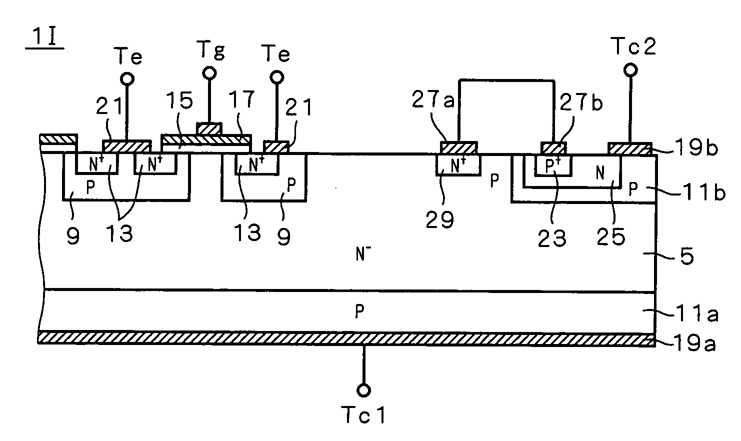
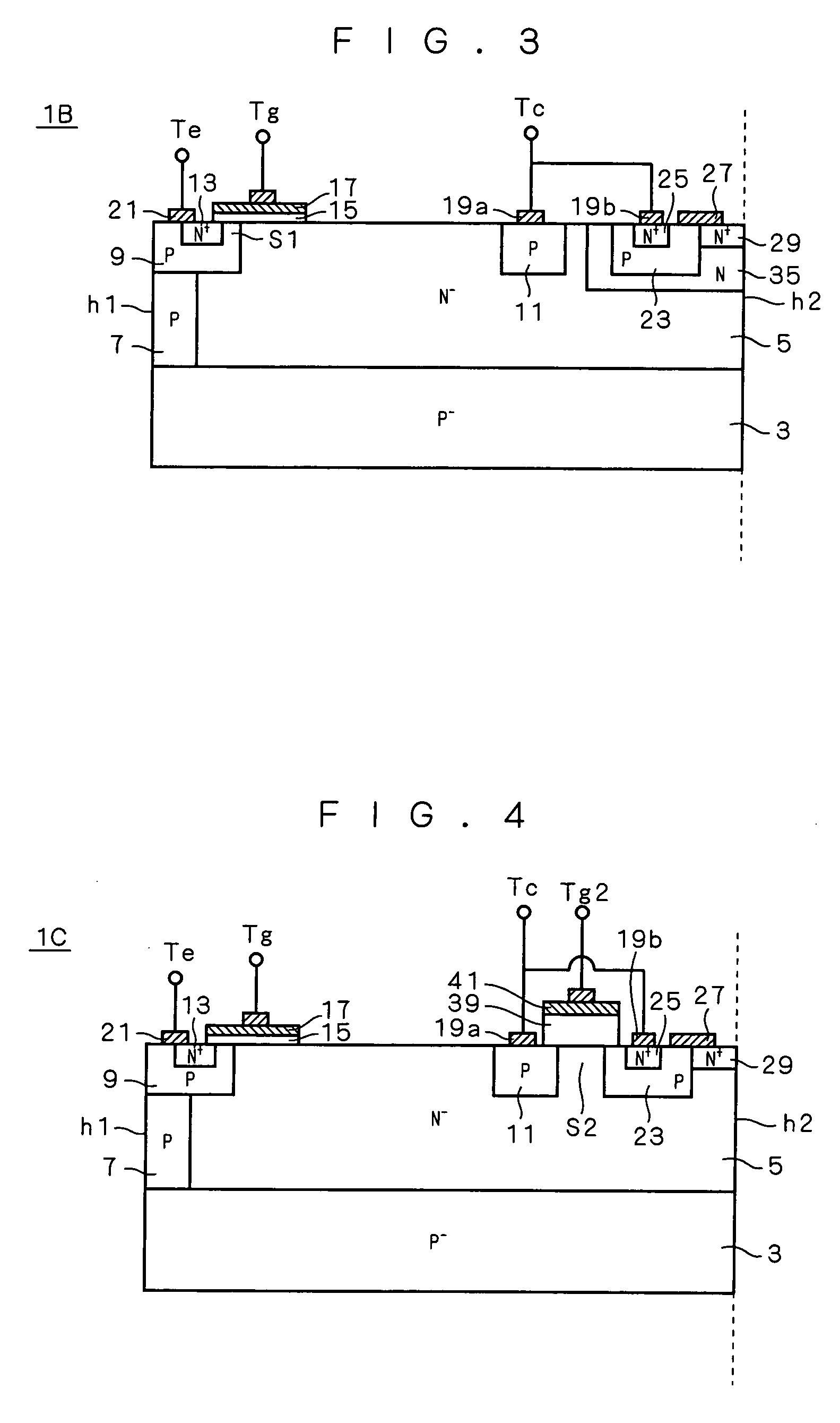
[0048] A semiconductor device 1B according to this preferred embodiment is, as shown in FIG. 3, constructed such that in the aforementioned first preferred embodiment, an N diffusion region (semiconductor region of the second conductivity type) 35 having a higher carrier density than the N− epitaxial layer 5 is further formed between the N− epitaxial layer 5 (semiconductor layer) and the P diffusion region 23 (fourth semiconductor region) to surround the P diffusion region 23.

[0049] In the semiconductor device 1A of the aforementioned first preferred embodiment, with reference to FIGS. 1 and 2, the formation of the diode D1 consisting of the components 23 and 25 for reverse conduction in the N− epitaxial layer 5 creates a parasitic PNP transistor whose emitter, base, and collector are formed respectively of the components 11, 5, and 23 (a dotted line 55 in FIG. 2 indicates the collector of this parasitic PNP transistor). When the collector terminal Tc is at a higher potential than ...

third preferred embodiment

[0051] A semiconductor device 1C according to this preferred embodiment is, as shown in FIG. 4, constructed such that in the aforementioned first preferred embodiment, a second gate electrode 41 is further provided on a surface portion of the N− epitaxial layer 5 (semiconductor layer) which is sandwitched between the P diffusion regions 11 and 23 (second and fourth semiconductor regions), with a second gate insulating film 39 in between; and a second gate terminal Tg2 is connected to the second gate electrode 41. That is, this semiconductor device 1C is such that a P-channel MOSFET Q2 (see FIG. 5) whose drain and source are formed respectively of the P diffusion regions 11 and 23 is further added to the aforementioned first preferred embodiment.

[0052] Here, the second gate insulating film 39 is formed to approximately a thickness of field oxide film so that the semiconductor device 1C can withstand high voltage.

[0053] The equivalent circuit of the semiconductor device 1C is, as sh...


PUM


Abstract

A semiconductor device includes a P diffusion region formed in the surface of an N epitaxial layer apart from other P diffusion regions; an N+ diffusion region formed in the surface of the P diffusion region so as to be surrounded by the P diffusion region; a second collector electrode provided on the N+ diffusion region and connected to a first collector electrode; and an electrode provided on and extending through the P diffusion region and the N epitaxial layer to form a conducting path from the Nepitaxial layer to the P diffusion region. This semiconductor device can improve both the operation and the reverse conducting capability of an IGBT.

Description

BACKGROUND OF THE INVENTION [0001] 1. Field of the Invention [0002] The present invention relates to a semiconductor device such as an integrated gate bipolar transistor (IGBT) and an integrated circuit (IC) with a built-in IGBT. [0003] 2. Description of the Background Art [0004] Generally, the equivalent circuit of a collector-shorted IGBT is structured such that the base and collector of a PNP transistor, between which the drain and source of an N-channel MOSFET are connected, are short-circuited via a resistance (first conventional example). [0005] In order to turn on the IGBT of this kind, when the collector of the IGBT (the emitter of the PNP transistor) is at a higher potential than the emitter of the IGBT (the source of the N-channel MOSFET), a predetermined positive voltage is applied to the gate of the IGBT (the gate of the N-channel MOSFET). Thereby, the N-channel MOSFET is turned on, whereby electrons are injected from the emitter of the IGBT through the N-channel MOSFET ...

Claims


Application Information

Patent Timeline
IPC IPC(8): H01L29/43
CPCH01L27/0647H01L29/7395H01L29/7393H01L29/70
Inventor TERASHIMA, TOMOHIDE
Owner MITSUBISHI ELECTRIC CORP
Why Eureka
Try Eureka