Supercharge Your Innovation With Domain-Expert AI Agents!

Semiconductor module

a technology of semiconductors and modules, applied in the direction of semiconductor devices, basic electric elements, resilient/clamping means, etc., can solve the problems of heat generation of power devices used in power sources, such as power mosfets, and achieve the effect of reducing the risk of heat generation

Inactive Publication Date: 2006-03-02
KK TOSHIBA
View PDF10 Cites 55 Cited by
  • Summary
  • Abstract
  • Description
  • Claims
  • Application Information

AI Technical Summary

Benefits of technology

The present invention provides a semiconductor module with improved heat dissipation and electrical connection between semiconductor chips. The module includes a mount member and two semiconductor chips mounted on the mount member with their upper surfaces facing the mount member. An electrically conductive and thermally radiative member connects the source electrode of one chip with the drain electrode of the other chip. A resinous member seals the chips in a single package. The first chip has a first semiconductor substrate, a first semiconductor region, a second semiconductor region, and a short electrode. The second chip has a second semiconductor substrate, a fourth semiconductor region, a fifth semiconductor region, and a sixth semiconductor region. The technical effects of the invention include improved heat dissipation, reduced power consumption, and improved electrical connection between semiconductor chips.

Problems solved by technology

A buttery or an AC source does not serve to supply power directly to the CPU and the CPU-controlled loads.
A power device for use in a power source, such as the power MOSFET, may produce heat due to power losses caused through the on-resistance and the switching operation.

Method used


Image

  • Semiconductor module
  • Semiconductor module
  • Semiconductor module

Examples


Embodiment Construction

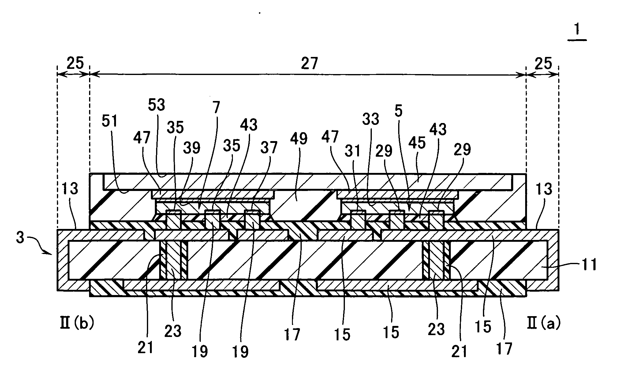
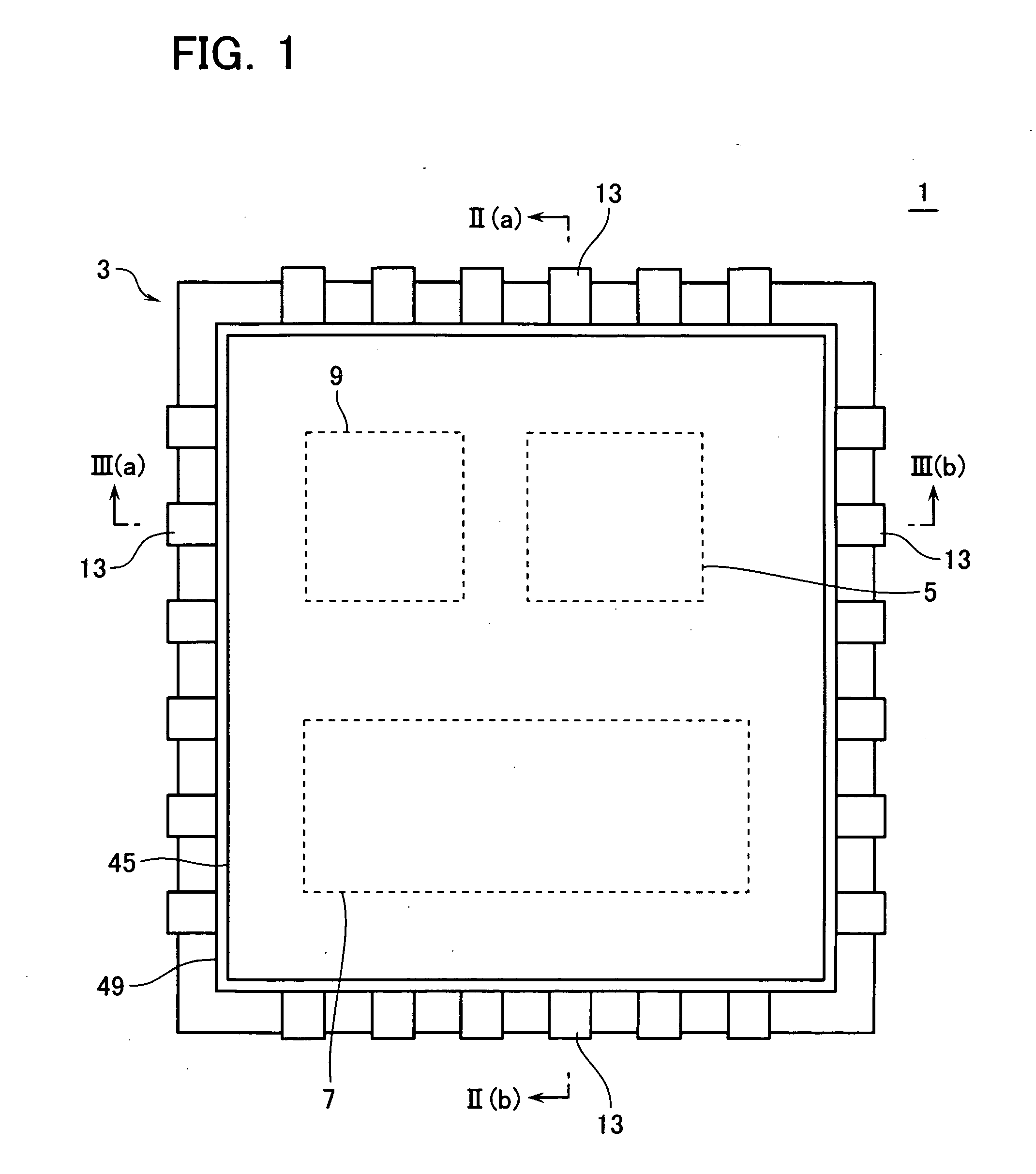
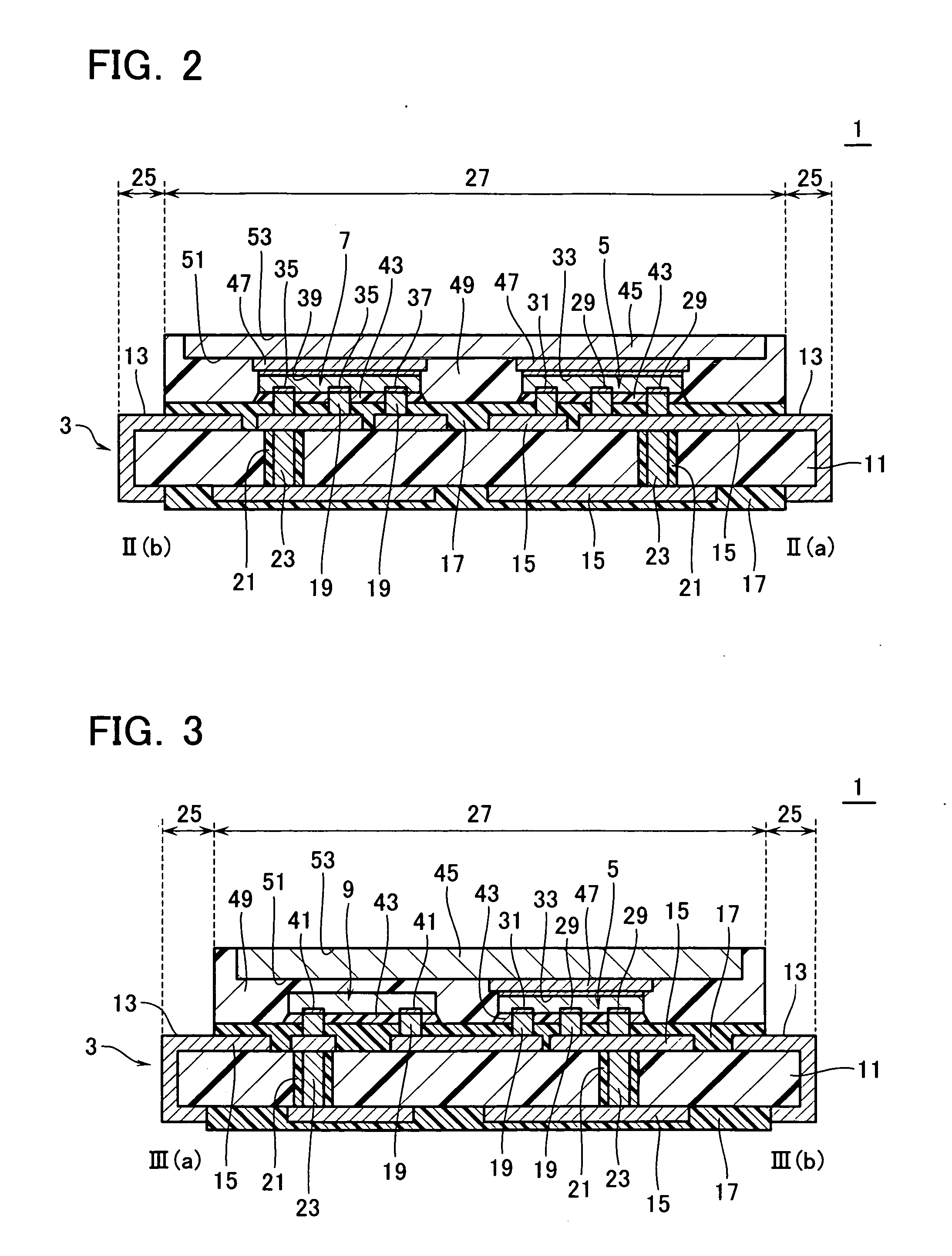
[0031] The embodiments of the present invention will now be described with reference to the drawings. In the figures illustrative of the embodiments, the same parts as those denoted with the reference numerals in the figure already described are denoted with the same reference numerals to omit their duplicated description. The semiconductor module according to the embodiment is exemplified as a multi-chip module that includes two power MOS chips and a driving IC chip all sealed in a single package. This module serves as part of a DC-DC converter.

[0032] The power MOS chip may comprise a FET that includes a gate insulator film composed of silicon oxide though the present invention is not limited to this example. For example, it is applicable to a power MIS (Metal Insulator Semiconductor) chip comprising a FET that includes a gate insulator film composed of an insulator other than silicon oxide (such as a high dielectric film). The power MOS chip is an example of the power MIS chip. T...


PUM


Abstract

A semiconductor module comprises a mount member. A first semiconductor chip having an upper surface and a lower surface is mounted via flip chip bonding on the mount member with the upper surface faced to the mount member. The upper surface includes a drain electrode and a gate formed therein and the lower surface includes a source electrode formed therein. A second semiconductor chip having an upper surface and a lower surface is mounted via flip chip bonding on the mount member with the upper surface faced to the mount member. The upper surface includes a source electrode and a gate formed therein and the lower surface includes a drain electrode formed therein. An electrically conductive and thermally radiative member is disposed to electrically connect the source electrode of the first semiconductor chip with the drain electrode of the second semiconductor chip and cover the lower surfaces of the semiconductor chips. A resinous member is provided to seal the first and second semiconductor chips in a single package.

Description

CROSS-REFERENCE TO RELATED APPLICATION [0001] This application is based upon and claims the benefit of priority from the prior Japanese Patent Application No. 2004-253140, filed on Aug. 31, 2004; the entire contents of which are incorporated herein by reference. BACKGROUND OF THE INVENTION [0002] 1. Field of the Invention [0003] The present invention relates to a semiconductor module such as a multi-chip module. [0004] 2. Description of the Related Art [0005] The use of a CPU in information communications instruments such as a personal computer strongly requires a lower voltage, a larger current and a faster response. The lower voltage serves to reduce power consumed in the CPU. The larger current is effective to achieve quick operation of the CPU and improve the integration density thereof. The faster response is advantageous to quickly respond to a variation in CPU-controlled load. In recent years, a CPU tends to have an operating voltage lowered to about 1 V, an operating current...

Claims


Application Information

Patent Timeline
Patent Type & Authority Applications(United States)
IPC IPC(8): H05K7/12
CPCH01L23/36H01L2924/13091H01L25/0655H01L2224/16225H01L2224/48091H01L2224/48247H01L2224/73265H01L2924/3011H01L23/3677H01L2924/30107H01L2924/12032H01L2224/73253H01L2224/32225H01L2224/73204H01L2924/00014H01L2924/00H01L2224/0557H01L2224/05573H01L2224/05571H01L2224/0554H01L25/072H01L2224/05599H01L2224/0555H01L2224/0556
Inventor MIURA, TAIKI
Owner KK TOSHIBA
Features
  • R&D
  • Intellectual Property
  • Life Sciences
  • Materials
  • Tech Scout
  • Unparalleled Data Quality
  • Higher Quality Content
  • 60% Fewer Hallucinations
Learn More