Optical Switch

a technology of optical switch and optical pulse, which is applied in the field of optical switch, can solve the problems of reducing the signal to noise ratio (s/n) of the optical pulse signal, increasing the propagation loss, and affecting the stability of the switching operation, so as to achieve stable switching operation independent

Inactive Publication Date: 2006-03-02
OKI ELECTRIC IND CO LTD
View PDF7 Cites 66 Cited by
  • Summary
  • Abstract
  • Description
  • Claims
  • Application Information

AI Technical Summary

Benefits of technology

[0025] It is therefore an object of the present invention to provide an optical switch that is capable of realizing a stable switching operation which is not affected even by variation in the polarization state of an input optical pulse signal serving as a control light. In other words, an object of the present invention is to provide an optical switch capable of realizing an operation that is stable enough for use in a 3R optical repeater or the like.
[0045] Hence, the respective contributions to the phase control amount of the signal light made by the two orthogonal polarization components of the control light input into the optical waveguide loop circuit through the control light input means are equalized by the wavelength demultiplexing / multiplexing circuit. Thus, according to the optical switch of the present invention, even if the polarization plane direction of the control light at the point of input into the optical waveguide loop circuit through the control light input means varies, the switching operation is not affected thereby, and a stable switching operation can be realized.
[0048] As will be described in detail hereafter, even when the duty ratio of the control light pulse is large, by disposing the phase bias circuit at a point on the optical waveguide loop circuit, this phase bias component can be removed. Thus, an optical switch which is capable of realizing a stable switching operation independent of the polarization state of the control light even when the duty ratio of the control light pulse is large can be constructed.

Problems solved by technology

This propagation loss increases steadily as the transmission distance increases.
Moreover, the chromatic dispersion of an optical fiber causes reductions in the signal to noise ratio (S / N) of the optical pulse signal and waveform distortion of the optical pulse signal, i.e. so-called waveform degradation of the optical pulse signal.
In an optical switch which uses the phenomenon of refractive index change caused by the optical Kerr effect, the fact that the amount of change in the refractive index depends on the relationship between the respective polarization directions of the signal light and control light leads to instability in the switching operation.
If a stable switching operation is not realized, the optical fiber loop cannot be used as an optical switch in a 3R optical repeater or the like.
Optical fiber transmission lines, which are used widely in optical communication and the like, are constituted by optical fiber which is not capable of maintaining the polarization state of the optical pulse signal that is propagated therethrough.
With a conventional optical switch using a NOLM, variation in the polarization state of the input optical pulse signal affects the switching operation such that a stable switching operation cannot be guaranteed.

Method used


Image

  • Optical Switch
  • Optical Switch
  • Optical Switch

Examples


first embodiment

[0065] (Structure)

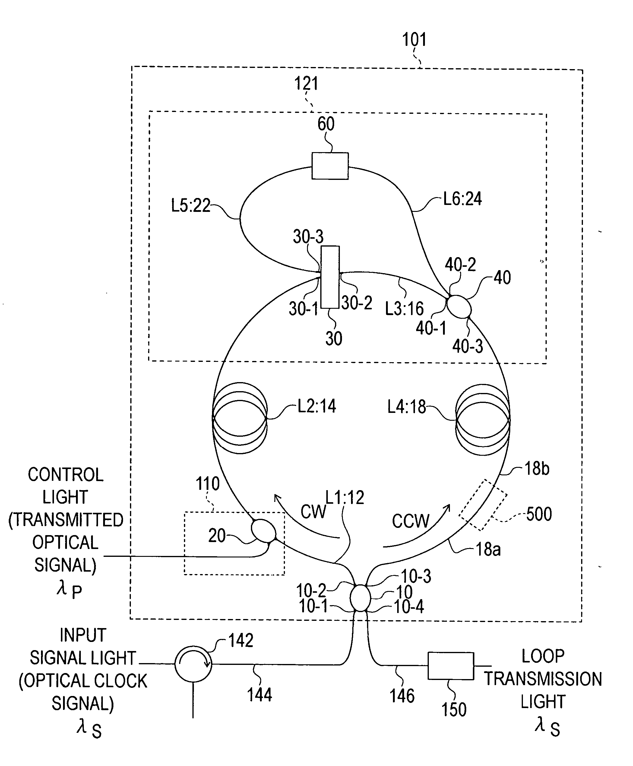
[0066] The structure of a first optical switch serving as a first embodiment of the present invention will now be described with reference to FIG. 1. The first optical switch is constituted by a loop-form optical waveguide loop circuit 101 formed from an optical nonlinear medium, and control light input means 20 of phase control means 110 for inputting a control light into the optical waveguide loop circuit 101, and also comprises a wavelength demultiplexing / multiplexing circuit 121 and a phase bias circuit 500.

[0067] The optical waveguide loop circuit 101 is constituted by an optical path (also referred to as “path L1” hereafter) formed from a first polarization-maintaining single-mode fiber 12 extending from an optical demultiplexer / multiplexer 10 to the control light input means 20, an optical path (also referred to as “path L2” hereafter) formed from a second polarization-maintaining single-mode fiber 14 extending from the control light input means 20 to the ...

second embodiment

[0221] (Structure)

[0222] The structure of a second optical switch serving as a second embodiment of the present invention will now be described with reference to FIG. 8. The second optical switch is constituted by a loop-form optical waveguide loop circuit 102 formed from an optical nonlinear medium, and the control light input means 20 of the phase control means 110 for inputting a control light into the optical waveguide loop circuit 102, and also comprises a wavelength demultiplexing / multiplexing circuit 122 and the phase bias circuit 500.

[0223] The constitution of the second optical switch differs from the constitution of the first optical switch described above in that an optical delay device 70 is inserted at a point on the path L6.

[0224] The optical demultiplexer / multiplexer 10 comprises the first port 10-1 for inputting a signal light, the second port 10-2 connected to one end of a first polarization-maintaining single-mode fiber 13, the third port 10-3 connected to the o...

third embodiment

[0258] (Structure)

[0259] The structure of a third optical switch serving as a third embodiment of the present invention will now be described with reference to FIG. 10. The third optical switch is constituted by a loop-form optical waveguide loop circuit 103 formed from an optical nonlinear medium, and the control light input means 20 of the phase control means 110 for inputting a control light into the optical waveguide loop circuit 103, and also comprises a wavelength demultiplexing / multiplexing circuit 123 and the phase bias circuit 500.

[0260] In the third optical switch, the optical waveguide loop circuit 103 is constituted by an optical path (also referred to as “path L1” hereafter) formed from the first polarization-maintaining single-mode fiber 13 extending from the optical demultiplexer / multiplexer 10 to the control light input means 20, an optical path (also referred to as “path L2” hereafter) formed from a second polarization-maintaining single-mode fiber 51 extending fr...


PUM

PropertyMeasurementUnit
wavelength bandwidthaaaaaaaaaa
temperatureaaaaaaaaaa
wavelengthaaaaaaaaaa

Abstract

The present invention provides an optical switch in which a switching operation is not affected even when the polarization state of a control light varies. The optical switch comprises a loop-form optical waveguide loop circuit formed from an optical nonlinear medium, control light input means of phase control means for inputting the control light into the optical waveguide loop circuit, a wavelength demultiplexing / multiplexing circuit, and a phase bias circuit. The optical waveguide loop circuit is constituted by an optical path formed from a first polarization-maintaining single-mode fiber extending from an optical demultiplexer / multiplexer to the control light input means, an optical path formed from a second polarization-maintaining single-mode fiber extending from the control light input means to the wavelength demultiplexing / multiplexing circuit, and an optical path formed from a fourth polarization-maintaining single-mode fiber extending from the wavelength demultiplexing / multiplexing circuit and returning to the optical demultiplexer / multiplexer. The wavelength demultiplexing / multiplexing circuit is formed as a loop-form optical waveguide loop circuit by a third polarization-maintaining single-mode fiber connecting a wavelength demultiplexer and a multiplexer, a fifth polarization-maintaining single-mode fiber connecting the wavelength demultiplexer and a polarization plane rotation portion, and a sixth polarization-maintaining single-mode fiber connecting the polarization plane rotation portion and the multiplexer. The phase bias circuit is inserted at a point on any one of the first through fourth polarization-maintaining single-mode fibers.

Description

BACKGROUND OF THE INVENTION [0001] 1. Field of the Invention [0002] The present invention relates to an optical switch used in long-distance, large capacity optical fiber communication and the like for switching a controlled light using a control light. [0003] 2. Description of Related Art [0004] To realize large capacity optical fiber communication using limited communication line resources effectively, means for increasing the number of channels capable of transmission and reception and means for increasing the communication speed must be provided. [0005] In optical fiber communication, communication is performed by propagating binary digital optical pulse signals, obtained by modulating an optical pulse array in which optical pulses are arranged in series, along an optical fiber serving as a transmission line at regular fixed time intervals. The term “regular fixed time intervals” denotes time intervals corresponding to the inverse of a frequency that corresponds to the bit rate....

Claims


Application Information

Patent Timeline
Patent Type & Authority Applications(United States)
IPC IPC(8): H04B10/00G02F1/365
CPCG02F1/3519
Inventor ARAHIRA, SHIN
Owner OKI ELECTRIC IND CO LTD
Why Eureka
Try Eureka