Method for manufacturing semiconductor device

a manufacturing method and semiconductor technology, applied in semiconductor devices, capacitors, electrical devices, etc., can solve the problems of difficult manufacturing of capacitors having longer durability and higher reliability without, and achieve the effect of enhancing the reliability of a semiconductor including a capacitor containing a capacitor dielectric film deposited by atomic layer deposition

Active Publication Date: 2006-03-02
RENESAS ELECTRONICS CORP
View PDF7 Cites 7 Cited by
  • Summary
  • Abstract
  • Description
  • Claims
  • Application Information

AI Technical Summary

Benefits of technology

[0010] As described later in the description of examples of the present invention, it has been clarified by the investigations of the present inventors that the reliability of the capacitor dielectric film can be enhanced by depositing the capacitor dielectric film via an atomic layer deposition within a certain temperature range centered on the above-described boundary temperature T (degree C.). Having such configuration, the reliability of the device employing such capacitor dielectric film can be enhanced.
[0017] According to the present invention, the reliability of a semiconductor including a capacitor containing a capacitor dielectric film deposited by the atomic layer deposition can be enhanced.

Problems solved by technology

However, as a result of investigations by the present inventors, it has been found that it is difficult to manufacture a capacitor having longer durability and higher reliability without an appropriate temperature control depending on the type of material, when a capacitor dielectric film is formed via ALD.

Method used


Image

  • Method for manufacturing semiconductor device
  • Method for manufacturing semiconductor device
  • Method for manufacturing semiconductor device

Examples


example 1

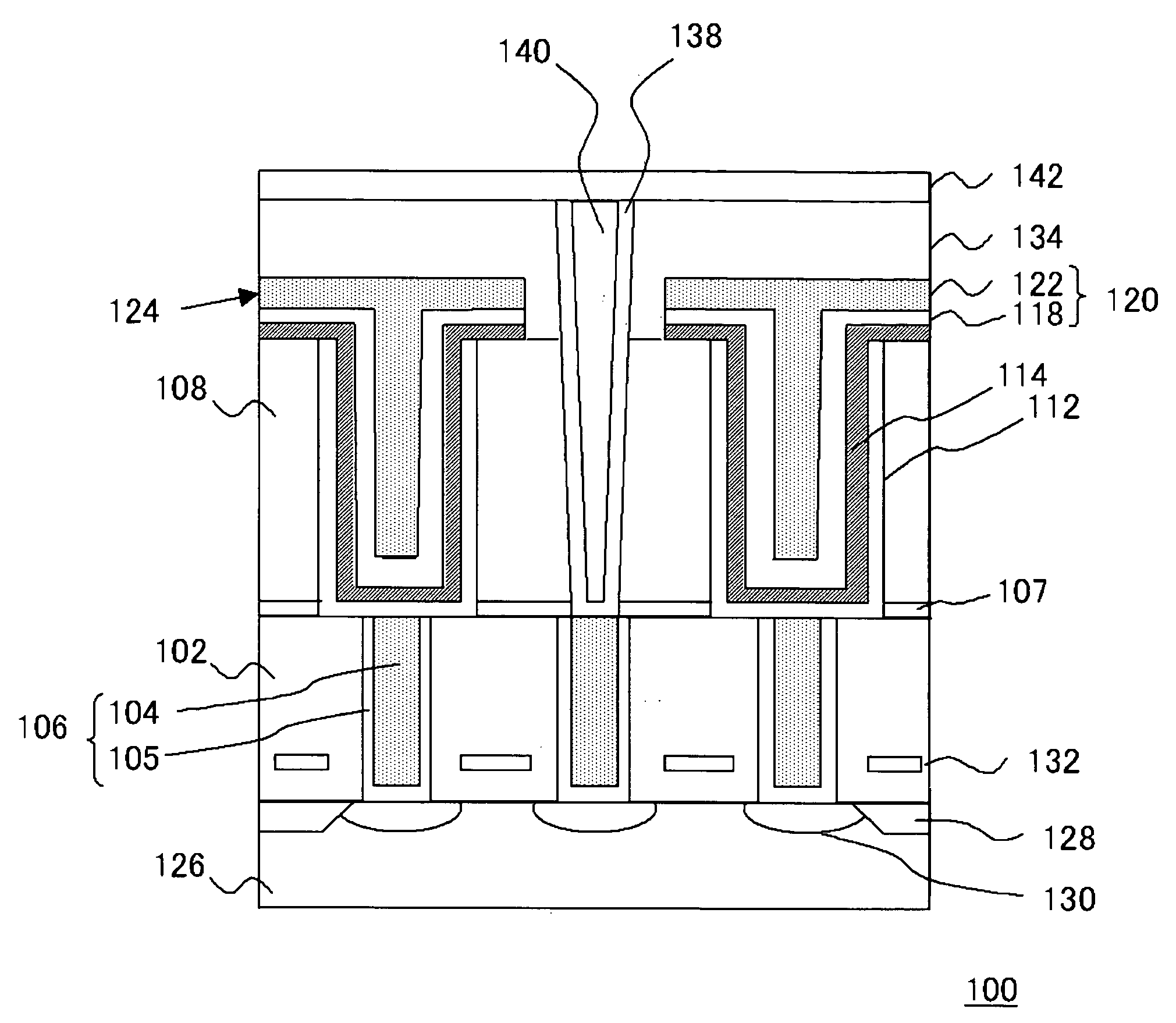
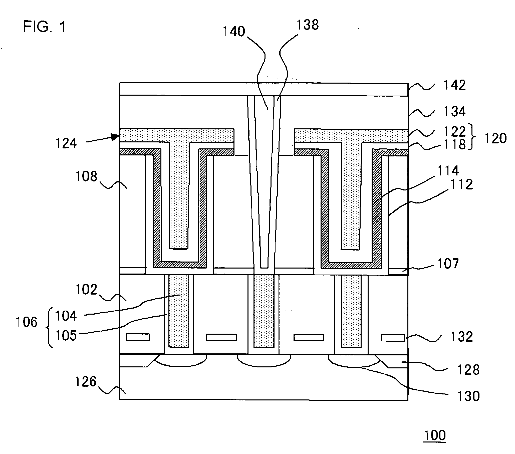
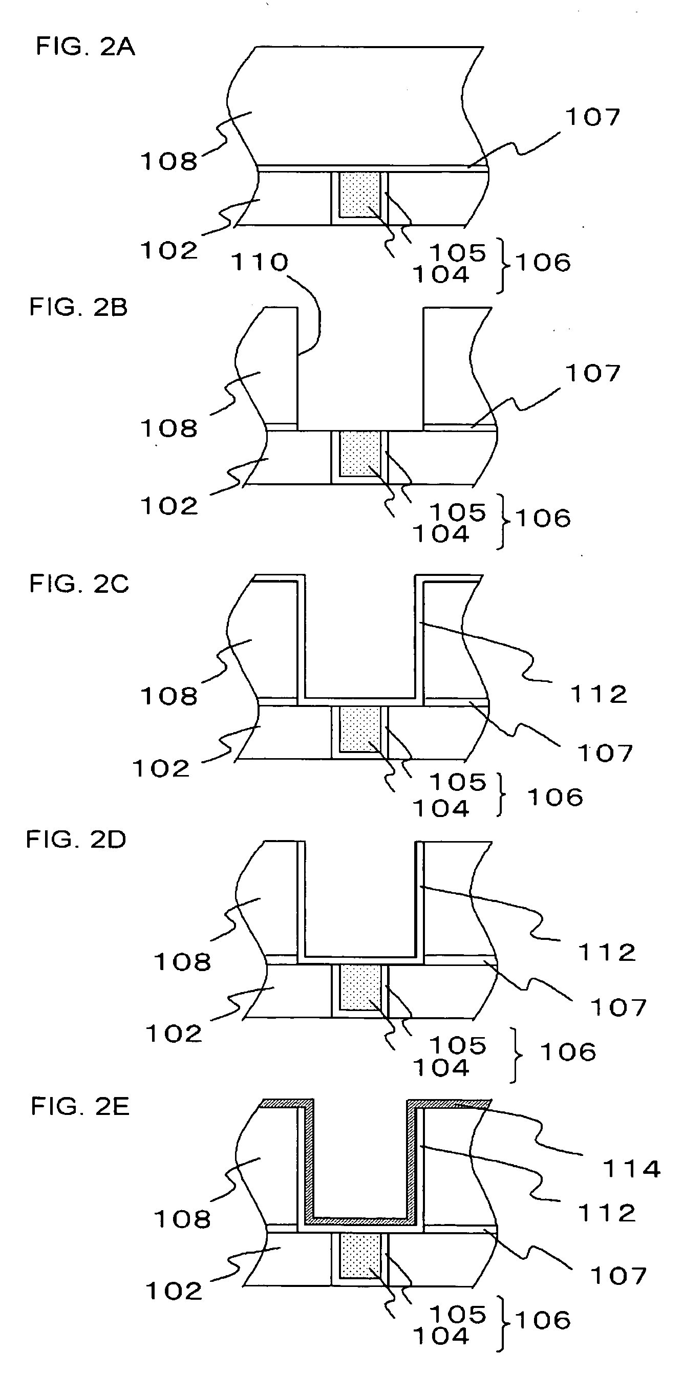
[0059] The capacitor dielectric film 114 composed of ZrO2 film was deposited by a method similar to that stated above to form the capacitor 124. Zr(N(Me)Et)4 (tetraethyl methylamino zirconium, TEMAZ) was employed for the deposition gas for depositing the capacitor dielectric film 114. O3 gas was employed for the oxidizing gas.

[0060] The correlation data between the deposition temperature and the thickness of the deposited film in every cycle in this case is shown in FIG. 6. In such case, the boundary temperature T (degree C.), at which an increase in a deposition rate in every cycle is shown, was 250 degree C.

[0061]FIG. 7 is a graph, showing results of a reliability test (time dependent dielectric breakdown, TDDB) of a capacitor 124 in the case that the thickness of the capacitor dielectric film 114 is 90 angstroms. The abscissa is assigned to a deposition temperature in depositing the capacitor 124, and the ordinate is assigned to a time required for breaking down more than half ...

example 2

[0065] The capacitor dielectric film 114 composed of HfO2 film was deposited by a method similar to that stated above to form the capacitor 124. Hf(N(Me)Et)4 (tetraethyl methylamino hafnium, TEMAH) was employed for the deposition gas. O3 gas was employed for the oxidizing gas.

[0066]FIG. 9 is a graph, showing the correlation data between the deposition temperature and the thickness of the deposited film in every cycle in the present example. In such case, the boundary temperature T (degree C.), at which an increase in a deposition rate in every cycle is shown, was 280 degree C.

[0067] The results of measuring the leakage current of the capacitors 124 including the capacitor dielectric films 14 deposited at the deposition temperatures of 280 degree C. and 310 degree C., respectively, are shown in FIG. 10. In such case, while lower leakage current of 1×10⁻¹⁶ (A / cell) was observed when the deposition was carried out at the boundary temperature of 280 degree C., when the deposition was ...


PUM

PropertyMeasurementUnit
thicknessaaaaaaaaaa
constant electrical voltageaaaaaaaaaa
temperatureaaaaaaaaaa

Abstract

In the process for manufacturing a semiconductor device of the present invention, a capacitor dielectric film is deposited via an atomic layer deposition employing an organic source material containing one or more metallic element(s) selected from the group consisting of Zr, Hf, La and Y as a deposition gas. The process for manufacturing a capacitor of the present invention includes obtaining a boundary temperature T (degree C.), at which an increase in a deposition rate for depositing the capacitor dielectric film as increasing the temperature is detected, on the basis of a correlation data of a deposition temperature in the atomic layer deposition employing the deposition gas with a deposition rate for depositing the capacitor dielectric film at the deposition temperature (S100 and S102); and depositing the capacitor dielectric film via the atomic layer deposition employing the deposition gas at a temperature within a range of from (T−20) (degree C.) to (T+20) (degree C.) (S104 to S112).

Description

[0001] This application is based on Japanese patent application NO. 2004-243284, the content of which is incorporated hereinto by reference. BACKGROUND OF THE INVENTION [0002] 1. Field of the Invention [0003] The present invention relates to a method for manufacturing a semiconductor device including a capacitor, and in particular, relates to a method for manufacturing a semiconductor device that utilize depositing a capacitor dielectric film of the capacitor by an atomic layer deposition. [0004] 2. Related Art [0005] Increasing achievements in miniaturization / integration of dynamic random access memory (DRAM) in recent years leads to promote a requirement for acquiring sufficient capacitance for a cell capacitance as one of critical issues. One of exemplary technique for acquiring sufficient capacitance may be a method of increasing a relative dielectric constant of a capacitor dielectric film. [0006] In Laid-Open Japanese Patent Application No. 2003-243,526, a capacitor including ...

Claims


Application Information

Patent Timeline
Patent Type & Authority Applications(United States)
IPC IPC(8): H01L21/20H01L21/8242H01L21/31
CPCH01L21/3141H01L21/31604H01L28/90H01L21/31645H01L27/10852H01L21/31641H01L21/02205H01L21/02175H01L21/0228H10B12/033
Inventor IINO, TOMOHISAFUKUMAKI, NAOMIKATO, YOSHITAKEYAMAMOTO, TOMOE
Owner RENESAS ELECTRONICS CORP
Why Eureka
Try Eureka