Image device and method of fabricating the same

a technology of image device and metal oxide semiconductor, which is applied in the field of image device, can solve the problems of affecting the performance of high-speed logic device, and copper cannot be easily etched, so as to improve light sensitivity, prevent scattering and irregular reflection of light, and improve light sensitivity

Inactive Publication Date: 2006-03-09
SAMSUNG ELECTRONICS CO LTD
View PDF16 Cites 35 Cited by
  • Summary
  • Abstract
  • Description
  • Claims
  • Application Information

AI Technical Summary

Benefits of technology

[0011] According to an embodiment of the present invention, an image device prevents scattering and irregular reflection of light. Thus light sensitivity can be improved.
[0012] According to an embodiment of the present invention, a method of fabricating an image device is disclosed. The method can simultaneously form a micro lens for improving light sensitivity when forming a dielectric layer comprising a transparent material for improving light transmittance.
[0013] According to an embodiment of the present invention, a method of fabricating an image device includes a simplified fabrication process.

Problems solved by technology

As a result, interconnection delay becomes more serious, thereby impeding performance of high-speed logic devices.
However, copper cannot be easily etched, and is prone to oxidation.

Method used


Image

  • Image device and method of fabricating the same
  • Image device and method of fabricating the same
  • Image device and method of fabricating the same

Examples


Embodiment Construction

[0032] Preferred embodiments of the present invention will be described below in more detail with reference to the accompanying drawings. The present invention may, however, be embodied in many different forms and should not be construed as being limited to the embodiments set forth herein. Like reference numerals refer to like elements throughout the specification.

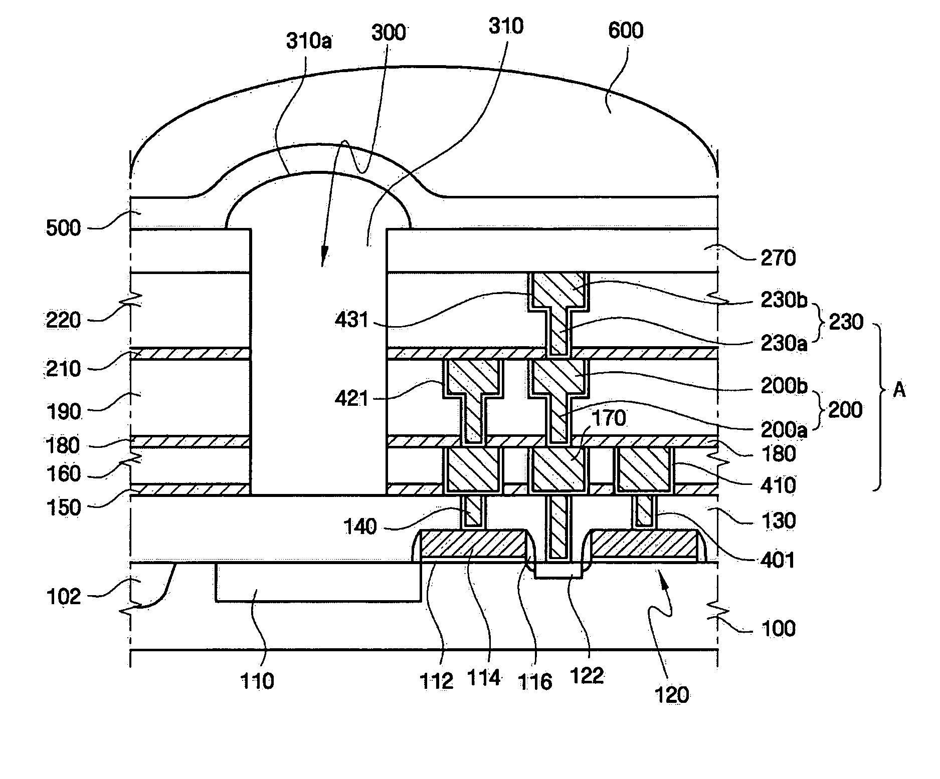
[0033] An image device according to an embodiment of the present invention will be described with reference to FIG. 1. FIG. 1 is a cross-sectional view of an image device according to an embodiment of the present invention.

[0034] As shown in FIG. 1, the image device according to an embodiment of the present invention includes a semiconductor substrate 100 having a light receiving element such as a photodiode 10 on a surface of an active region defined by a field oxide layer 102. Transistors 120, which are switching devices, are formed on the semiconductor substrate 100. The transistors 120 include a gate electrode 114, ...


PUM


Abstract

An image device includes a substrate in which a light receiving element is formed, an interlayer dielectric structure which is formed on the substrate and has a cavity over the light receiving element, a transparent dielectric layer which fills the cavity and has a lens-shaped portion protruding beyond an upper portion of the interlayer dielectric structure, and a color filter which is formed on the transparent dielectric layer.

Description

CROSS-REFERENCE TO RELATED APPLICATIONS [0001] This application claims priority to Korean Patent Application No. 10-2004-0071761 filed on Sep. 8, 2004 in the Korean Intellectual Property Office, the disclosure of which is incorporated herein by reference in its entirety. BACKGROUND OF THE INVENTION [0002] 1. Technical Field [0003] The present disclosure relates to an image device and a method of fabricating the same, and more particularly, to a complementary metal oxide semiconductor (CMOS) image device fabricated using a copper damascene process and a method of fabricating the same. [0004] 2. Discussion of Related Art [0005] A CMOS image sensor includes a light sensing part for sensing light and a logic circuit part for converting sensed light into an electronic signal and converting the electronic signal into data. To increase light sensitivity, an effort has been made to increase a ratio of an area occupied by the light sensing part in the CMOS image sensor. [0006] With progress ...

Claims


Application Information

Patent Timeline
Patent Type & Authority Applications(United States)
IPC IPC(8): H01L31/062H01L21/768H01L27/14H01L27/146H04N5/335H04N5/369H04N5/374
CPCH01L27/14609H01L27/14621H01L27/14625H01L27/14687H01L27/14636H01L27/14643H01L27/14685H01L27/14627H01L27/146H01L31/10
Inventor OH, HYEOK-SANGCHUNG, JU-HYUCKPARK, KWANG-MYEONCHO, IN-SOOKIM, SEONG-IL
Owner SAMSUNG ELECTRONICS CO LTD
Why Eureka
Try Eureka