Electrostatic discharge protection circuit

Inactive Publication Date: 2006-03-09
WINBOND ELECTRONICS CORP
View PDF13 Cites 23 Cited by
  • Summary
  • Abstract
  • Description
  • Claims
  • Application Information

AI Technical Summary

Benefits of technology

[0027] In brief, the present invention provides a plurality of clamping circuits each comprising a series of bipolar transistors connected in stack. Thus, gate over-drive problem in the MOS transistor of the bypass circuit is prevented. Furthermore, the present invention also provides a lower conductive resistance and voltage surge

Problems solved by technology

However, as the dimensions of integrated circuits (IC) are gradually reduced, the tolerance of current diminishes correspondingly.
Therefore, the smaller the size of integrated circuits, the larger the damages caused by electrostatic discharge (ESD).
Hence, if the integrated circuit receives electrostatic discharge suddenly, the integrated circuit may be burnt, damaged or punched through.
However, the performance of the ESD protection circuit shown in FIG. 1 is generally poor because the turn-on speed is rather slow.
One major drawback of the aforementioned techniques shown in FIGS. 2 and 3 is

Method used


Image

  • Electrostatic discharge protection circuit
  • Electrostatic discharge protection circuit
  • Electrostatic discharge protection circuit

Examples


Embodiment Construction

[0035] Reference will now be made in detail to the present preferred embodiments of the invention, examples of which are illustrated in the accompanying drawings. Wherever possible, the same reference numbers are used in the drawings and the description to refer to the same or like parts.

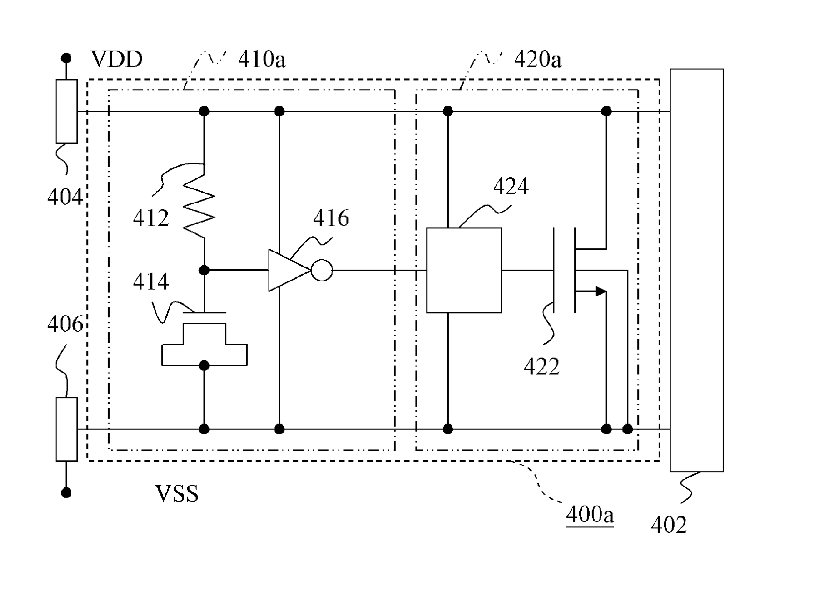
[0036]FIGS. 4A, 4B and 4C are schematic circuit diagrams illustrating an electrostatic discharge protection circuit according to one embodiment of the present invention. As shown in FIG. 4A, the ESD protection circuit 400a may comprise a detection circuit 410a and a bypass circuit 420a. The detection circuit 410a is connected to a first pad 404, a second pad 406 and an integrated circuit 402, and may be adopted for detecting an ESD current. The bypass circuit 420a is connected to the first pad 404, the second pad 406 and the output terminal of the detection circuit 410a, and may be adopted for bypassing the ESD current. In one embodiment of the present invention, the first pad 404 is connected to a...


PUM


Abstract

An ESD protection circuit includes a detection circuit for detecting an ESD current and a bypass circuit for bypassing the ESD. The detection circuit and bypass circuit are connected to a first pad and a second pad. The bypass circuit is connected to an output terminal of the detection circuit. The bypass circuit comprises a MOS transistor, a first bipolar transistor and a second bipolar transistor. The drain of the MOS transistor, the collectors of the first bipolar transistor and the collector of the second bipolar transistor are connected to the first pad. The source and the substrate of the MOS transistor and the emitter of the second bipolar transistor are connected to the second pad. The base of the first bipolar transistor is connected to the gate of the MOS transistor and the emitter of the first bipolar transistor is connected to the base of the second bipolar transistor.

Description

BACKGROUND OF THE INVENTION [0001] 1. Field of the Invention [0002] The present invention relates to an electrostatic discharge protection circuit. More particularly, the present invention relates to an electrostatic discharge protection circuit with a bypass circuit having a plurality of bipolar transistors connected in stack. [0003] 2. Description of the Related Art [0004] In recent years, the integration of semiconductor devices advances by reducing the line width and increasing the number of stacked film layers. For example, in the metal-oxide-semiconductor (MOS) devices, the thickness of the gate oxide layer is reduced and the length of the channel is shortened as the MOS device is miniaturized. Furthermore, thickness of the junction between source and drain is reduced and the source / drain region is fabricated using the lightly doped drain (LDD) method. However, as the dimensions of integrated circuits (IC) are gradually reduced, the tolerance of current diminishes correspondin...

Claims


Application Information

Patent Timeline
IPC IPC(8): H02H9/00
CPCH02H9/046
Inventor JEN-CHOU, TSENG
Owner WINBOND ELECTRONICS CORP
Why Eureka
Try Eureka