Piezoelectric element and head for jetting liquid and method for manufacturing them

Inactive Publication Date: 2006-03-09
SEIKO EPSON CORP
View PDF8 Cites 0 Cited by
  • Summary
  • Abstract
  • Description
  • Claims
  • Application Information

AI Technical Summary

Benefits of technology

[0011] In the first aspect, when the lowermost layer of the piezoelectric layers is formed, the rate of temperature increase while degreasing is maintained relatively low, thus forming a number of small seed crystals within the lowermost layer of the piezoelectric layers. Thus, the piezoelectric film with a favorable film quality can be formed.
[0041] In the sixteenth aspect, ejection properties are improved and also become uniform, thus realizing the liquid jet head with improved reliability.

Problems solved by technology

In the conventional degreasing step in manufacturing the piezoelectric element, nucleuses of piezoelectric crystals in the precursor of the piezoelectric film has not been easily formed.
Therefore, it has been difficult to obtain desired crystals when the precursor is crystallized.
Moreover, when forming the piezoelectric film on the lower electrode which is patterned as mentioned earlier, a problem arises that portions of the piezoelectric film formed to cover edges of the lower electrode and other portion of the same formed on the outer sides of the lower electrode have poor film qualities, and thereby a drive reliability of the piezoelectric element is degraded.
Thus, the piezoelectric layer is substantially discontinuous in the vicinities of edges of the lower electrode thereby causing breakage such as a crack in the piezoelectric film when a voltage is applied thereto.

Method used


Image

  • Piezoelectric element and head for jetting liquid and method for manufacturing them
  • Piezoelectric element and head for jetting liquid and method for manufacturing them
  • Piezoelectric element and head for jetting liquid and method for manufacturing them

Examples


embodiment 1

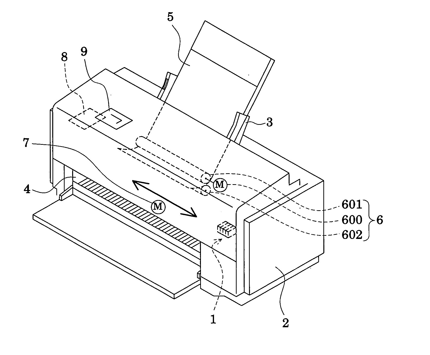
[0059]FIG. 1 is an explanatory view of a construction of a printer (an example of a liquid jet device) using an ink-jet recording head (an example of a liquid jet head) which is provided with a piezoelectric element manufactured in a method of this embodiment. This printer is provided with a body 2, a tray 3, a discharge port 4 and an operation panel 9. In addition, the ink-jet recording head 1, a feeding mechanism 6 and a control circuit 8 are provided within the body 2.

[0060] The ink-jet recording head 1 is provided with the piezoelectric element manufactured in the manufacturing method of the present invention. The ink-jet recording head 1 is constructed to be able to eject ink, which is a liquid, from a nozzle in accordance with an ejection signal supplied from the control circuit 8.

[0061] The body 2 is a casing of the printer, in which the feeding mechanism 6 is placed at the position where paper 5 can be fed from the tray 3, and the ink-jet recording head 1 is placed to be a...

embodiment 2

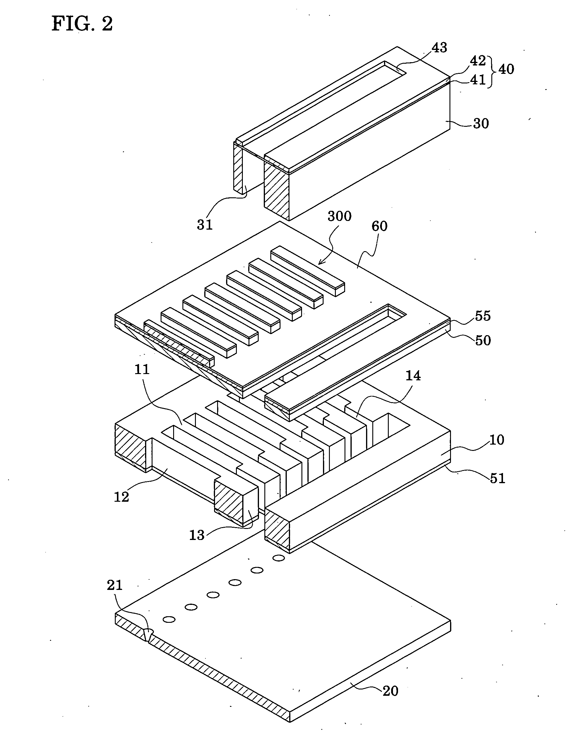
[0090]FIG. 8 is an exploded perspective view schematically showing an ink-jet recording head according to Embodiment 2 of the present invention. FIGS. 9(a) and 9(b) are a plan view of FIG. 8 and a cross-sectional view taken along the line B-B′, respectively. FIG. 10 is a schematic view showing a layer construction of a piezoelectric element. Note that the same members as those described in Embodiment 1 are denoted by the same referential numerals, and duplicated description is thus omitted.

[0091] This embodiment is another example of the layer construction of the piezoelectric element. Specifically, as shown in FIGS. 8 to 10, the a lower electrode film 60A constructing the piezoelectric element 300 is patterned in the vicinities of both edges of each pressure generating chamber 12 and continuously provided along a direction in which the pressure generating chamber 12 is provided. Moreover, in this embodiment, each end face of the lower electrode film 60A in a region facing each of ...

embodiment 3

[0110] FIGS. 16(a) and 16(b) are a plan view and a cross-sectional view of an ink-jet recording head according to Embodiment 3.

[0111] This embodiment is an example in which metal layers are provided on a vibration plate in the vicinities of edges of a piezoelectric film 70A. This construction is same as that of Embodiment 2 except provision of the metal layers. Specifically, as shown in FIGS. 16(a) and 16(b), metal layers 61 are provided in the vicinities of both edges of the piezoelectric film 70A in a longitudinal direction thereof. The metal films 61 are formed in the same layer of the lower electrode film 60A, but are electrically disconnected from the lower electrode film 60A. The piezoelectric film 70A is provided, extending over a part of each metal layers 61.

[0112] Note that, in this embodiment, a metal film 61A is provided in the vicinity of the edge of the piezoelectric film 70A on the side of the lead electrode 90. The metal film 61A is also provided separately for each...


PUM


Abstract

Provided are a piezoelectric element in which favorable crystallinity can be obtained with improved uniformity, breakage of a piezoelectric film can be prevented, and thereby stable displacement properties can be obtained, a liquid-jet head using the piezoelectric element and a manufacturing method thereof. Steps of forming a piezoelectric layer are carried out a plurality of times so that a plurality of the piezoelectric layers are stacked, thus forming the piezoelectric film. The steps of forming the piezoelectric layer include: applying a sol containing an organometallic compound, drying the sol containing the organometallic compound, degreasing the sol containing the organometallic compound thus gelating the sol, and crystallizing the gelated organometallic compound. When forming a lowermost layer of the piezoelectric layers, a rate of temperature increase at least during initial degreasing is set to be 500° C. / min or lower.

Description

TECHNICAL FIELD [0001] The present invention relates to a piezoelectric element and a liquid jet head using the same, and particularly to a manufacturing method of the piezoelectric element, which can make a crystal orientation within a wafer surface uniform, thus making piezoelectric properties of the piezoelectric element uniform. BACKGROUND ART [0002] A piezoelectric element is an element in which a piezoelectric film, having an electromechanical transducing function, is sandwiched by two electrodes. The piezoelectric film is made of crystallized piezoelectric ceramics. [0003] Conventionally, a so-called sol-gel method has been known as a manufacturing method of the piezoelectric element. Specifically, a sol of an organometallic compound is applied on a substrate in which a lower electrode is formed, and then the sol is dried and degreased to form a precursor film of a piezoelectric layer. After the steps of application, drying and degreasing of the sol is carried out predetermin...

Claims


Application Information

Patent Timeline
IPC IPC(8): H01L21/8234B41J2/16H01L41/09H01L41/318H01L41/39
CPCB41J2/161B41J2/1623B41J2/1628B41J2/1645H01L41/318B41J2002/14419B41J2002/14491H01L41/0973H01L41/1876B41J2002/14241H10N30/2047H10N30/8554H10N30/078
Inventor MURAI, MASAMI
Owner SEIKO EPSON CORP
Why Eureka
Try Eureka