

Circuit board and method of manufacturing the same
a technology of circuit boards and conductive patterns, applied in the field of circuit boards, can solve the problems of large impedances of conductive patterns for high-frequency signals, and achieve the effect of small impedances
- Summary
- Abstract
- Description
- Claims
- Application Information
AI Technical Summary
Benefits of technology
Problems solved by technology
Method used
Image

Examples
exemplary embodiment 1
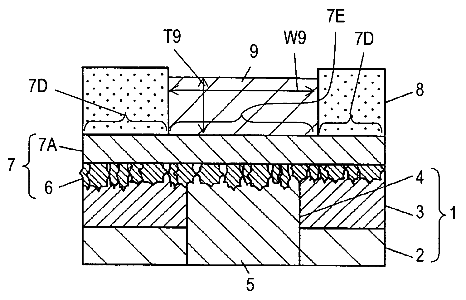
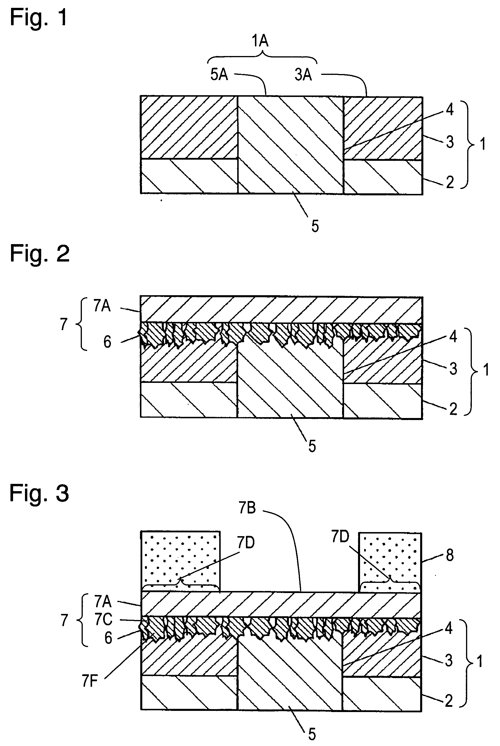
[0022] FIGS. 1 to 6 are cross sectional views of a circuit board for illustrating processes of manufacturing the circuit board according to Exemplary Embodiment 1 of the present invention.
[0023]FIG. 1 is a cross sectional view of insulating substrate 1 having through hole 4 filled with conductive material 5. Fiber sheet 2 of glass cloth (glass fabric) woven with insulating fiber, such as aramid resin fiber or glass fiber has both surfaces each impregnated with epoxy resin to provide resin layer 3 having a thickness ranging, for example, from 5 μm to 20 μm. Insulating substrate 1, or a glass epoxy substrate, is thus provided. Through-hole 4 is formed in insulating substrate 1 by optical process, such as CO2 gas laser, or a mechanical drill. Through-hole 4 is filled with a paste of electro conductive material 5 provided by mixing 30-80 vol. % of copper grains having diameters of 1 μm to 50 μm in a resin material for a 30-80 capacitive %, by printing process or injection.
[0024] Later...
exemplary embodiment 2
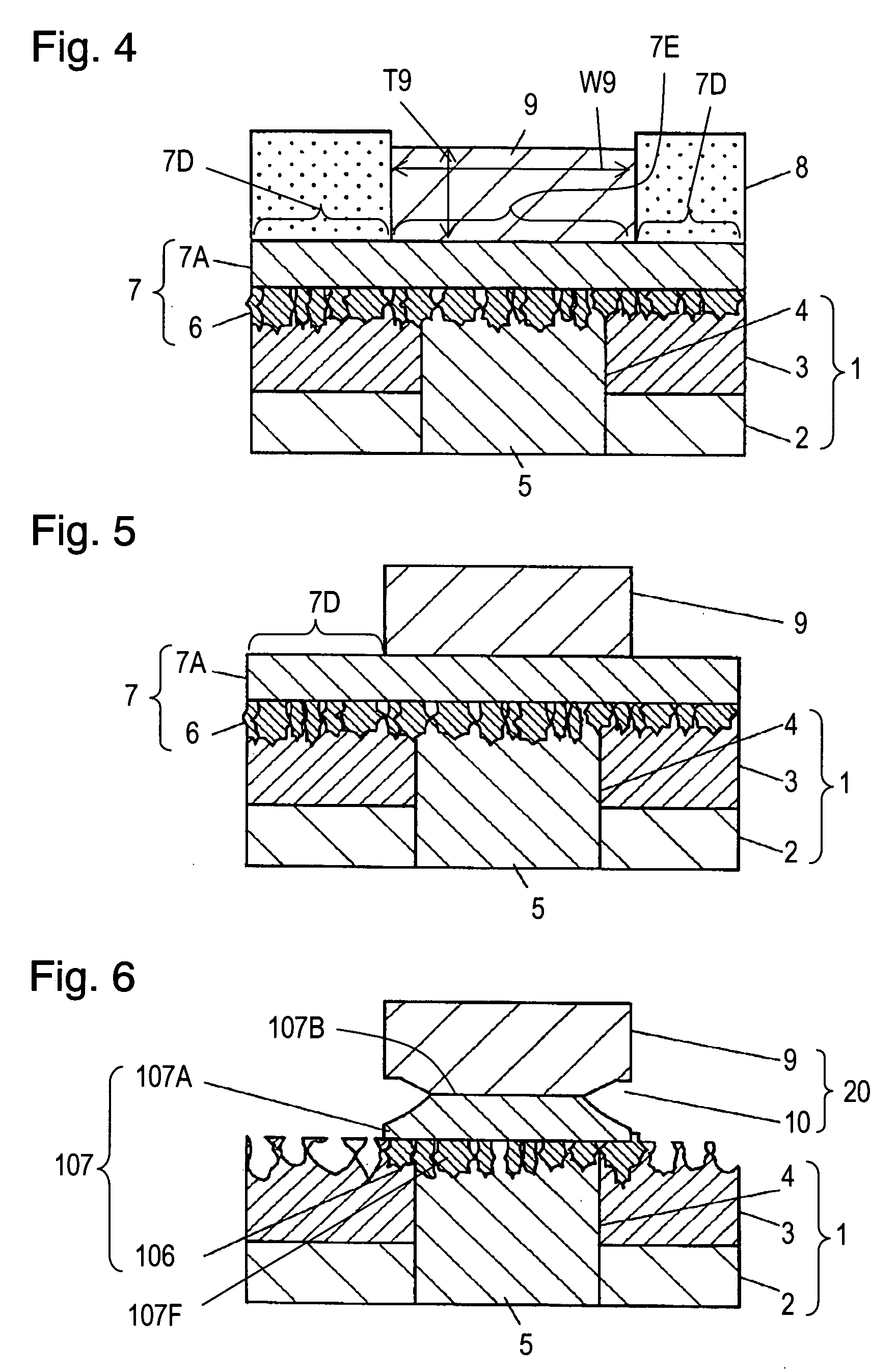
[0047] FIGS. 8 to 15 are cross sectional views of a circuit board for illustrating a method of manufacturing the circuit board according to Exemplary Embodiment 2 of the present invention. Portions identical to those of Embodiment 1 are denoted by the same reference numerals, and description of the portions is eliminated.
[0048] First, as shown in FIG. 8, insulating substrate 1 formed by the same method as of the Embodiment 1 is provided with through-hole 4 by an optical method, such as CO2 gas laser or by a mechanical method, such as drilling. Through-hole 4 is filled with paste of electrical conductive material 5. Conductive material is provided by mixing 30 to 80 vol. % of copper grains having diameters ranging from 1 μm to 50 μm in resin material. The paste can be dispensed by printing process or jet nozzle injection.
[0049] As shown in FIG. 9, rough layer 506 is provided on surface of 501A of insulating substrate 1 by applying a roughening process, i.e., on surface 505A of cond...
PUM
| Property | Measurement | Unit |
|---|---|---|
| thickness | aaaaa | aaaaa |
| diameters | aaaaa | aaaaa |
| diameter | aaaaa | aaaaa |
Abstract
Description
Claims
Application Information