Phosphorus activated NMOS using SiC process

a technology of phosphorus and nmos, applied in the direction of semiconductor devices, electrical apparatus, transistors, etc., can solve the problems of non-abrupt junctions, adversely affecting channel characteristics, and high diffusivity of phosphorus, so as to mitigate the proclivity of phosphorus and high activity. , the effect of high activity

Active Publication Date: 2006-03-23
TEXAS INSTR INC
View PDF12 Cites 12 Cited by
  • Summary
  • Abstract
  • Description
  • Claims
  • Application Information

AI Technical Summary

Benefits of technology

[0006] The present invention relates to a device and method of fabrication, wherein a transistor device exhibits a high level of activity due to the use of phosphorus as a source / drain dopant. One or more portions of a silicon substrate upon which the device is formed are treated to include carbon which mitigates the proclivity of phosphorus to diffuse. In this manner, a transistor device having a high level of activity is produced having more abrupt junctions. As such, channel characteristics, injection velocity, carrier mobility and / or drive current are thereby enhanced. Further, the carbon within the substrate may produce a tensile stress therein which may further enhance mobility and lower channel resistance.

Problems solved by technology

However, phosphorus has a high diffusity which can lead to non-abrupt junctions.
Non-abrupt junctions can be detrimental to the performance of the transistor by adversely affecting channel characteristics, injection velocity, carrier mobility and / or drive current.

Method used


Image

  • Phosphorus activated NMOS using SiC process
  • Phosphorus activated NMOS using SiC process
  • Phosphorus activated NMOS using SiC process

Examples


Embodiment Construction

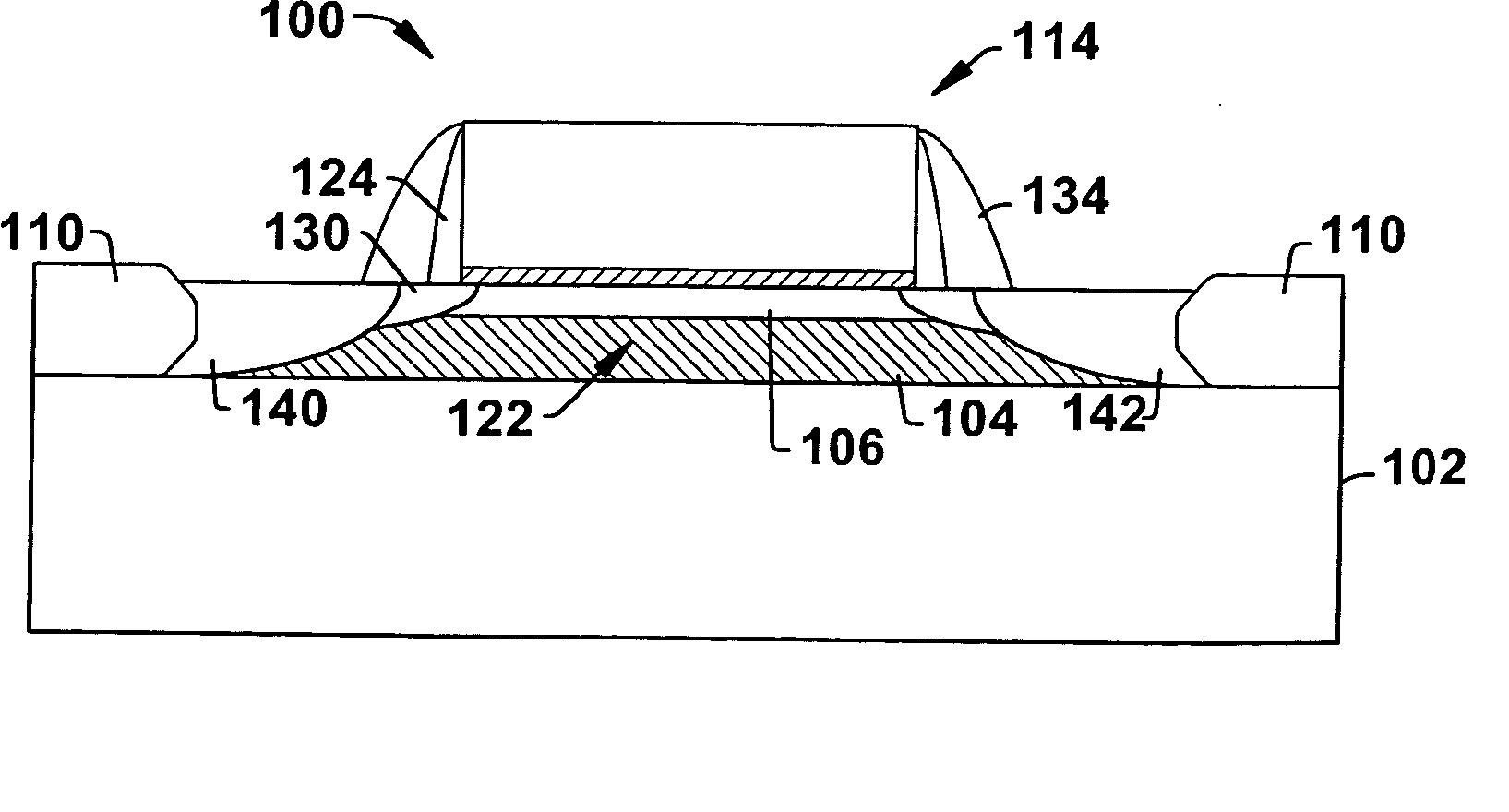
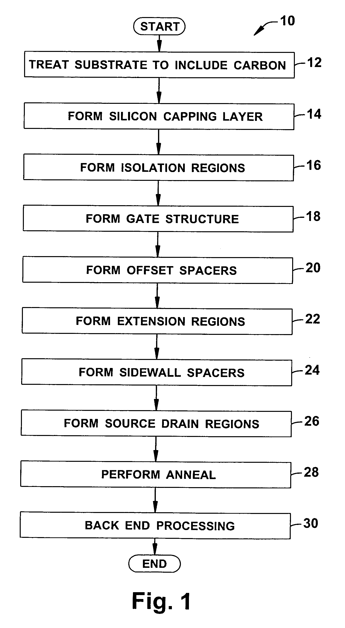
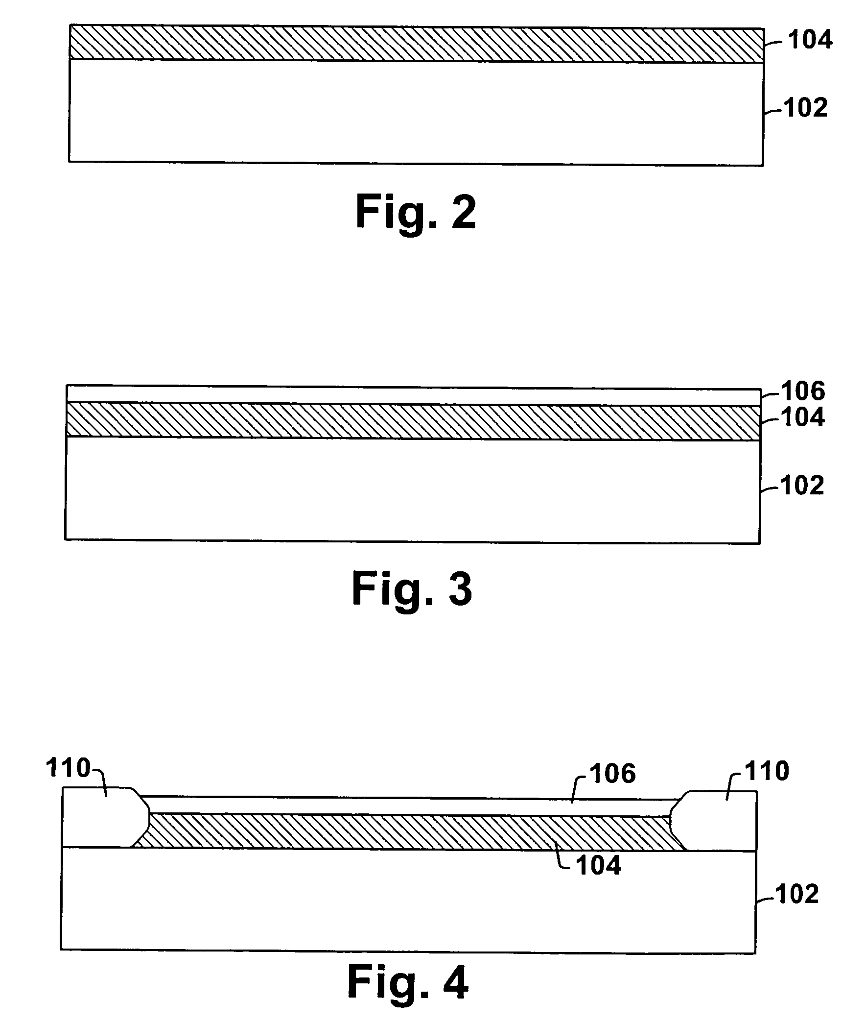
[0016] One or more aspects of the present invention are described with reference to the drawings, wherein like reference numerals are generally utilized to refer to like elements throughout, and wherein the various structures are not necessarily drawn to scale. It will be appreciated that where like acts, events, elements, layers, structures, etc. are reproduced in the Figs., subsequent (redundant) discussions of the same may be omitted for the sake of brevity. In the following description, for purposes of explanation, numerous specific details are set forth in order to provide a thorough understanding of one or more aspects of the present invention. It may be evident, however, to one of ordinary skill in the art that one or more aspects of the present invention may be practiced with a lesser degree of these specific details. In other instances, known structures are shown in diagrammatic form in order to facilitate describing one or more aspects of the present invention.

[0017] The ...


PUM


Abstract

A method (10) of forming a transistor (100) includes treating (12) at least some of a semiconductor substrate (102) with carbon and then forming (18) a gate structure (114) over the semiconductor substrate. A channel region (122) is thereby being defined within the semiconductor substrate (102) below the gate structure (114). Source and drain regions (140, 142) are then formed (26) within the semiconductor substrate (102) on opposing sides of the channel (122) with a phosphorus dopant.

Description

FIELD OF INVENTION [0001] The present invention relates generally to semiconductor fabrication and more particularly to utilizing a phosphorus dopant in a semiconductor substrate that has been treated to include silicon carbon material in a transistor fabrication process. BACKGROUND OF THE INVENTION [0002] A conventional MOS transistor generally includes a semiconductor substrate, such as silicon, having a gate structure or gate stack formed thereover. The gate structure comprises a conductive gate electrode overlying a thin gate dielectric. The gate electrode typically includes polysilicon and the gate dielectric an oxide based material. Source and drain regions are formed in the substrate substantially aligned with the gate structure. The source and drain regions are generally formed by applying a dopant to the select regions of the substrate. A channel is defined within the substrate under the gate structure between the source and drain regions. [0003] A voltage applied to the ga...

Claims


Application Information

Patent Timeline
Patent Type & Authority Applications(United States)
IPC IPC(8): H01L29/80
CPCH01L29/1054H01L29/165H01L29/66651H01L29/6659H01L29/66636H01L29/6656
Inventor CHAKRAVARTHI, SRINIVASANCHIDAMBARAM, P.R.
Owner TEXAS INSTR INC
Why Eureka
Try Eureka