Integrated nanotube and field effect switching device

a nanotube and field effect technology, applied in nanoelectromechanical switches, pulse techniques, instruments, etc., can solve the problems of high power consumption, density and operation speed of mos digital circuits, and limited density of bipolar digital integrated circuits

Active Publication Date: 2006-03-23
NANTERO
View PDF98 Cites 90 Cited by
  • Summary
  • Abstract
  • Description
  • Claims
  • Application Information

AI Technical Summary

Benefits of technology

[0039] Embodiments of the present invention provide integrated switching devices that combine nanotube (NT) switching elements with field effect semiconductor elements, including but not limited to M

Problems solved by technology

However, the density of bipolar digital integrated circuits is limited by their high power consumption and the ability of packaging technology to dissipate the heat produced while the circuits are operating.
The density and operating speed of MOS digital circuits are still limited by the need to dissipate the heat produced when the device is operating.
Digital logic integrated circuits constructed from bipolar or MOS devices do not function correctly under conditions of high heat or heavy radiation.
As leakage current increases, the operating temperature of the device rises, the power consumed by the circuit increases, and the difficulty of discriminating the off state from the on state reduces circuit reliability.
Conventional digital logic circuits also short internally when subjec

Method used


Image

  • Integrated nanotube and field effect switching device
  • Integrated nanotube and field effect switching device
  • Integrated nanotube and field effect switching device

Examples


Embodiment Construction

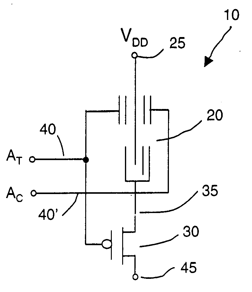
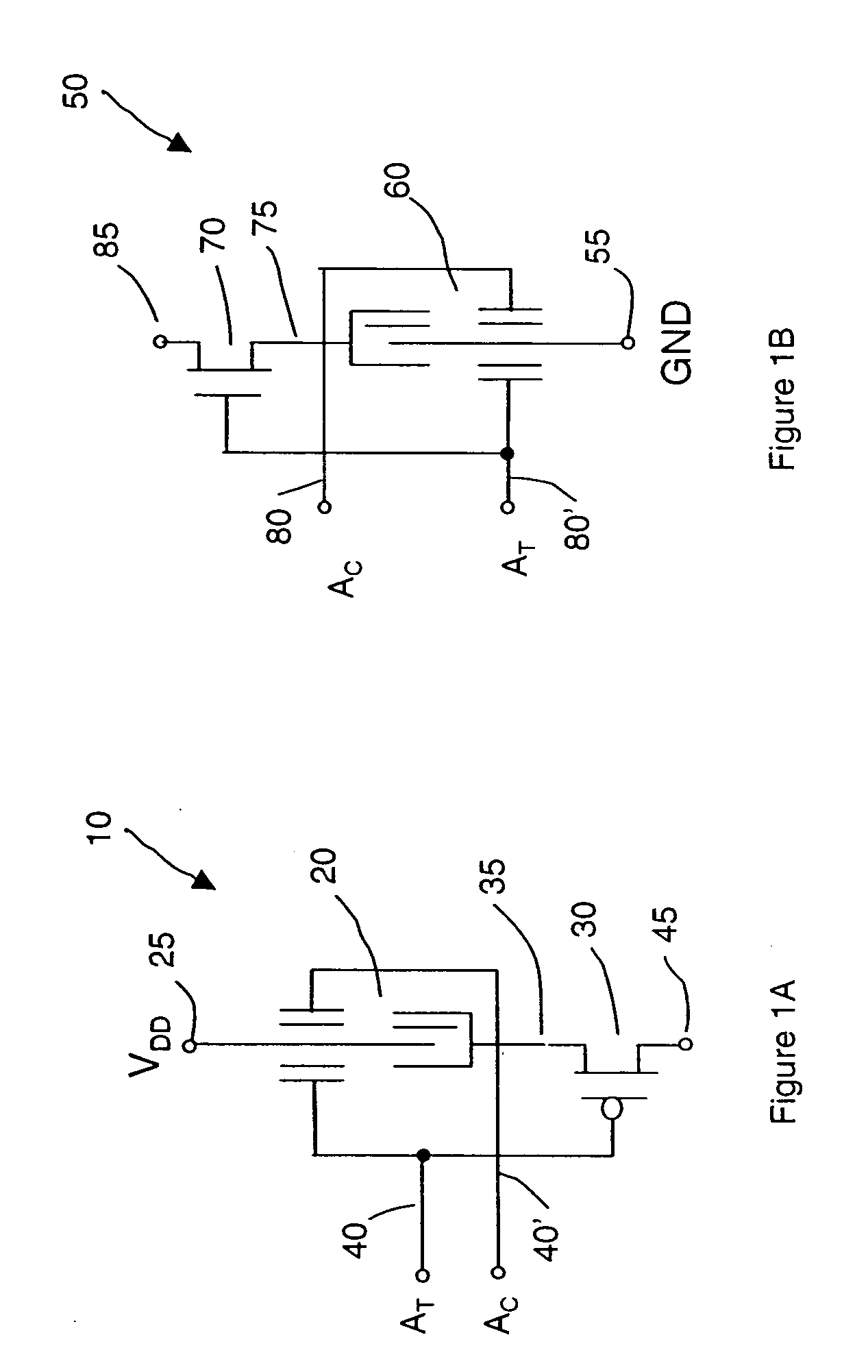
[0058] Embodiments of the invention provide switching elements with a conductive channel that has both a nanotube component and a field effect semiconductor component. Preferred embodiments of the invention provide integrated hybrid logic devices that use nanotube switching elements in combination with field effect devices resembling field effect transistors (FETs). The integrated devices are referred to herein as NT-FET devices. The NT-FET devices of preferred embodiments form an NT-FET device family. The devices in the NT-FET device family can be used as switching elements and to implement any desired logic function or logical device, such as an inverter. In certain embodiments, an NT-FET device includes a MOSFET, e.g., a p-channel FET (PFET) or an n-channel FET (NFET), placed in series with a nanotube switching element connected to a source (VDD or GND). In preferred embodiments, the gate of the FET is logically tied to a control input of the nanotube switching element. In some e...


PUM


Abstract

Hybrid switching devices integrate nanotube switching elements with field effect devices, such as NFETs and PFETs. A switching device forms and unforms a conductive channel from the signal input to the output subject to the relative state of the control input. In embodiments of the invention, the conductive channel includes a nanotube channel element and a field modulatable semiconductor channel element. The switching device may include a nanotube switching element and a field effect device electrically disposed in series. According to one aspect of the invention, an integrated switching device is a four-terminal device with a signal input terminal, a control input terminal, a second input terminal, and an output terminal. The devices may be non-volatile. The devices can form the basis for a hybrid NT-FET logic family and can be used to implement any Boolean logic circuit.

Description

CROSS-REFERENCE TO RELATED APPLICATIONS [0001] This application claims priority under 35 U.S.C. § 119(e) to U.S. Provisional Pat. Apl., Ser. No. 60 / 581,015, filed on Jun. 18, 2004, entitled Nonvolatile Carbon Nanotube Logic (NLOGIC) and CMOS Inverter, which is incorporated herein by reference in its entirety. [0002] This application is related to the following applications: [0003] U.S. patent application Ser. No. 10 / 917,794, filed on Aug. 13, 2004, entitled Nanotube-Based Switching Elements; [0004] U.S. patent application Ser. No. 10 / 918,085, filed on Aug. 13, 2004, entitled Nanotube-Based Switching Elements With Multiple Controls; [0005] U.S. patent application Ser. No. 10 / 918,181, filed on Aug. 13, 2004, entitled Nanotube Device Structure And Methods Of Fabrication; [0006] U.S. patent application Ser. No. 10 / 917,893, filed on Aug. 13, 2004, entitled Nanotube-Based Switching Elements And Logic Circuits; [0007] U.S. patent application Ser. No. 10 / 917,606, filed on Aug. 13, 2004, ent...

Claims


Application Information

Patent Timeline
IPC IPC(8): H03K19/20
CPCB82Y10/00G11C13/025G11C23/00G11C2213/17Y10S977/94H03K17/545H03K19/08Y10S977/70H01H1/0094
Inventor BERTIN, CLAUDE L.
Owner NANTERO
Why Eureka
Try Eureka