Apparatus and process for surface treatment of substrate using an activated reactive gas
a technology of activated reactive gas and apparatus, which is applied in the direction of coating, chemical vapor deposition coating, electric discharge tube, etc., can solve the problems of inability to implement plasma activation of reactive gas system for treating wide and/or long surface areas of materials precisely, uniformly and reproducibly, and the treatment of plasma activation of reactive gas system has, so far, been limited to small surface areas
- Summary
- Abstract
- Description
- Claims
- Application Information
AI Technical Summary
Problems solved by technology
Method used
Image
Examples
example 1
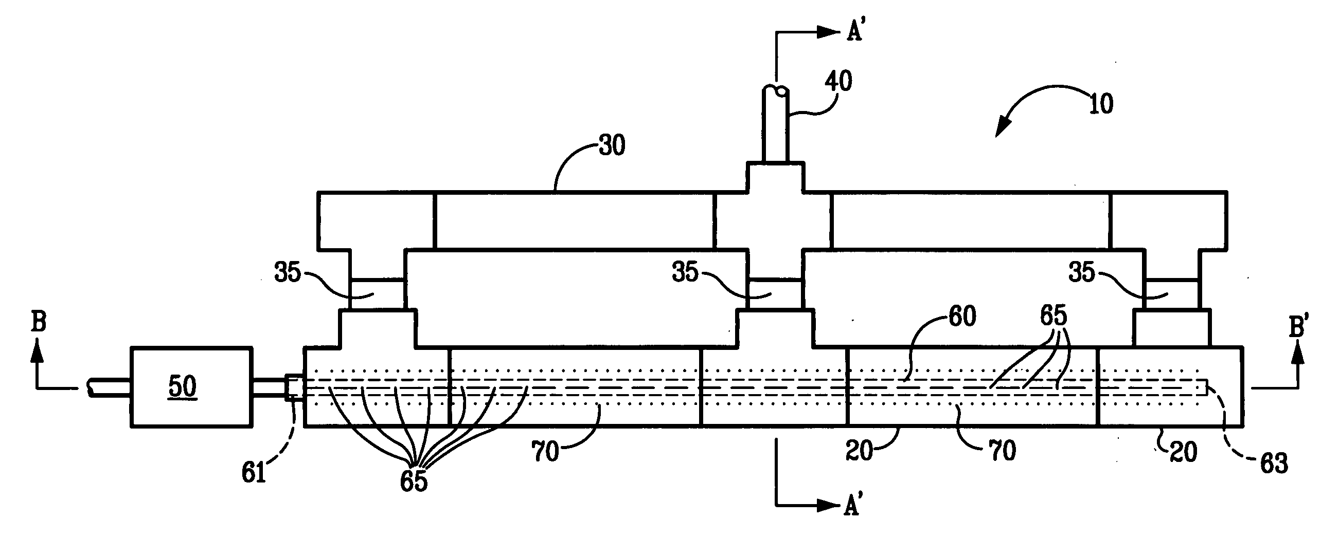
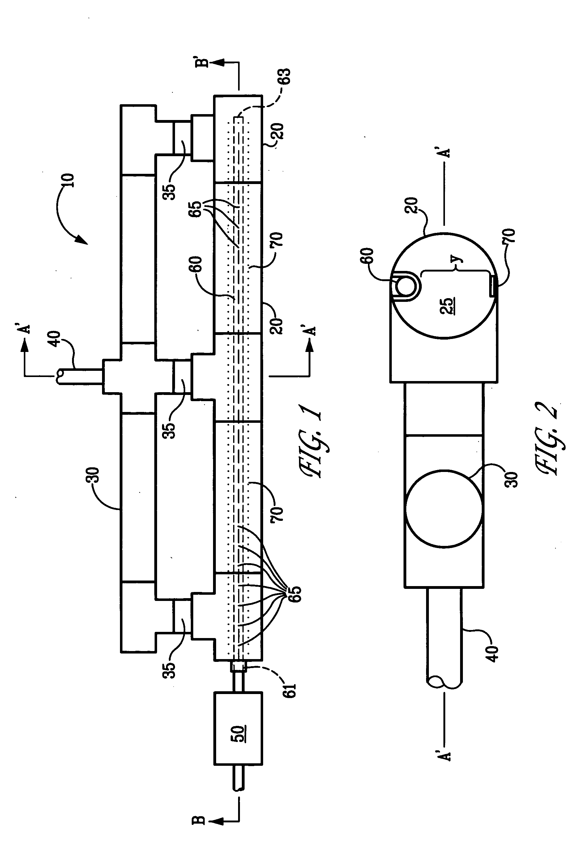
[0038] The vacuum processing chamber described above was used to treat the surface of two 4″ diameter silicon wafers that were thermally treated in the presence of an oxygen-containing gas to provide an approximately 470 nanometer (nm) thick silicon oxide layer with an average root mean square (rms) surface roughness of approximately 0.43 nm. The wafers were placed within the vacuum processing chamber in a location that was 8 inches and 7.5 feet from the entrance of the activated gas into the processing chamber, respectively, to approximate the extreme ends of the processing chamber. The wafers were placed on the two extreme ends to simulate treatment of an approximately 8 foot wide substrate surface. The processing chamber was operated at a pressure of about 1.4 torr. The distribution pipe was supplied with a 1000 standard cubic centimeter per minute (sccm) flow of NF3 gas that was activated using the external RF plasma source described above. The distance of wafers from the openin...
example 2
[0039] The surface treatment of two 4″ diameter silicon wafers with approximately 470 nanometer (nm) thick silicon oxide layer described in Example 1 was repeated in the same vacuum chamber with similar placement of wafers. The vacuum chamber was operated at a pressure of about 0.94 torr instead of using 1.4 torr pressure. The distribution pipe was supplied with a 3000 standard cubic centimeter per minute (sccm) flow of NF3 gas that was activated using the external RF plasma source described above. The distance of wafers from the opening was approximately 6 inches. These wafers were exposed to activated NF3 gas for a total time of 2 minutes. Thereafter, the flow of activated NF3 gas was terminated, the distribution pipe and vacuum chamber were purged with argon gas, and the treated wafers were removed for analysis. The analytical results showed that from about 60 to about 90 nm of silicon oxide layer was removed from these wafers. The surface roughness of silicon oxide layer was not...
example 3
[0040] The surface treatment of two 4″ diameter silicon wafers with approximately 470 nanometer (nm) thick silicon oxide layer described in Example 1 was repeated in the same vacuum chamber with similar placement of wafers. The vacuum chamber was operated at a pressure of about 1.4 torr. The distribution pipe was supplied with a 3000 standard cubic centimeter per minute (sccm) flow of NF3 gas that was activated using the external RF plasma source described above. The distance of wafers from the opening was approximately 2 inches instead of using 6 inches. These wafers were exposed to activated NF3 gas for a total time of 3 minutes. Thereafter, the flow of activated NF3 gas was terminated, the distribution pipe and vacuum chamber were purged with argon gas, and the treated wafers were removed for analysis. The analytical results showed that from about 120 to about 250 nm of silicon oxide layer was removed from these wafers. The surface roughness of silicon oxide layer was noted to be...
PUM
| Property | Measurement | Unit |
|---|---|---|
| Length | aaaaa | aaaaa |
| Energy | aaaaa | aaaaa |
Abstract
Description
Claims
Application Information


