Semiconductor device, method of measuring light intensity distribution of laser light, laser annealing apparatus, and crystallization method

a semiconductor and light intensity distribution technology, applied in the direction of optical radiation measurement, instruments, manufacturing tools, etc., can solve the problems of insufficient light intensity distribution, poor physical properties of polycrystalline silicon (poly-si) films, and inability to accurately image the light intensity distribution (plane image)

Inactive Publication Date: 2006-03-30
ADVANCED LCD TECH DEVMENT CENT
View PDF7 Cites 0 Cited by
  • Summary
  • Abstract
  • Description
  • Claims
  • Application Information

AI Technical Summary

Benefits of technology

[0016] The present invention has been developed in view of the above-described problems concerning a conventional method of measuring light intensity distribution of laser light. An object of the present invention is to provide a semicond

Problems solved by technology

However, the amorphous silicon film has a disadvantage that the film is inferior to a polycrystalline silicon (poly-Si) film in physical properties such as conductivity.
However, a method of correctly imaging the light intensity distribution (plane image) is very difficult, and has not been established yet in the present conditions.
There are fluctuations in the material itself that causes the physical property changes, it is therefore very difficult to grasp the light intensi

Method used


Image

  • Semiconductor device, method of measuring light intensity distribution of laser light, laser annealing apparatus, and crystallization method
  • Semiconductor device, method of measuring light intensity distribution of laser light, laser annealing apparatus, and crystallization method
  • Semiconductor device, method of measuring light intensity distribution of laser light, laser annealing apparatus, and crystallization method

Examples


example 1

A Substrate to be Treated, on Whose Whole Surface a Light-Emitting Layer is Formed

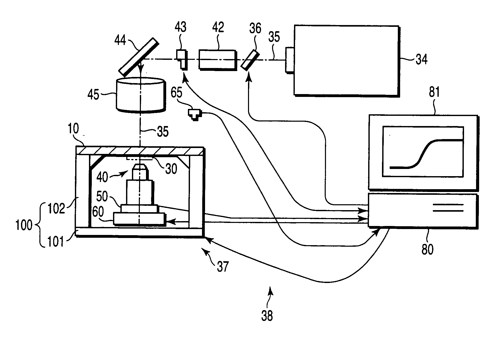
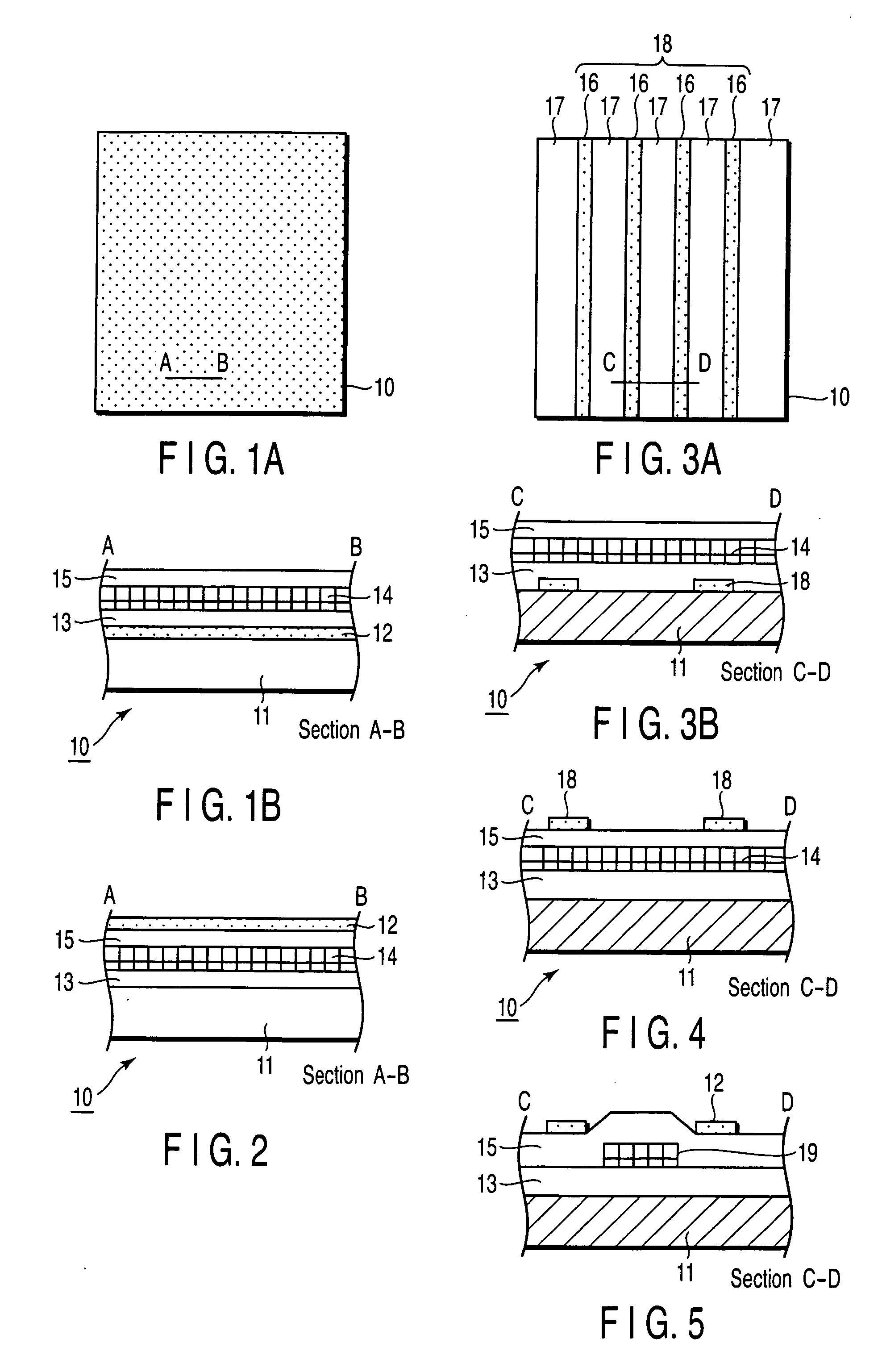
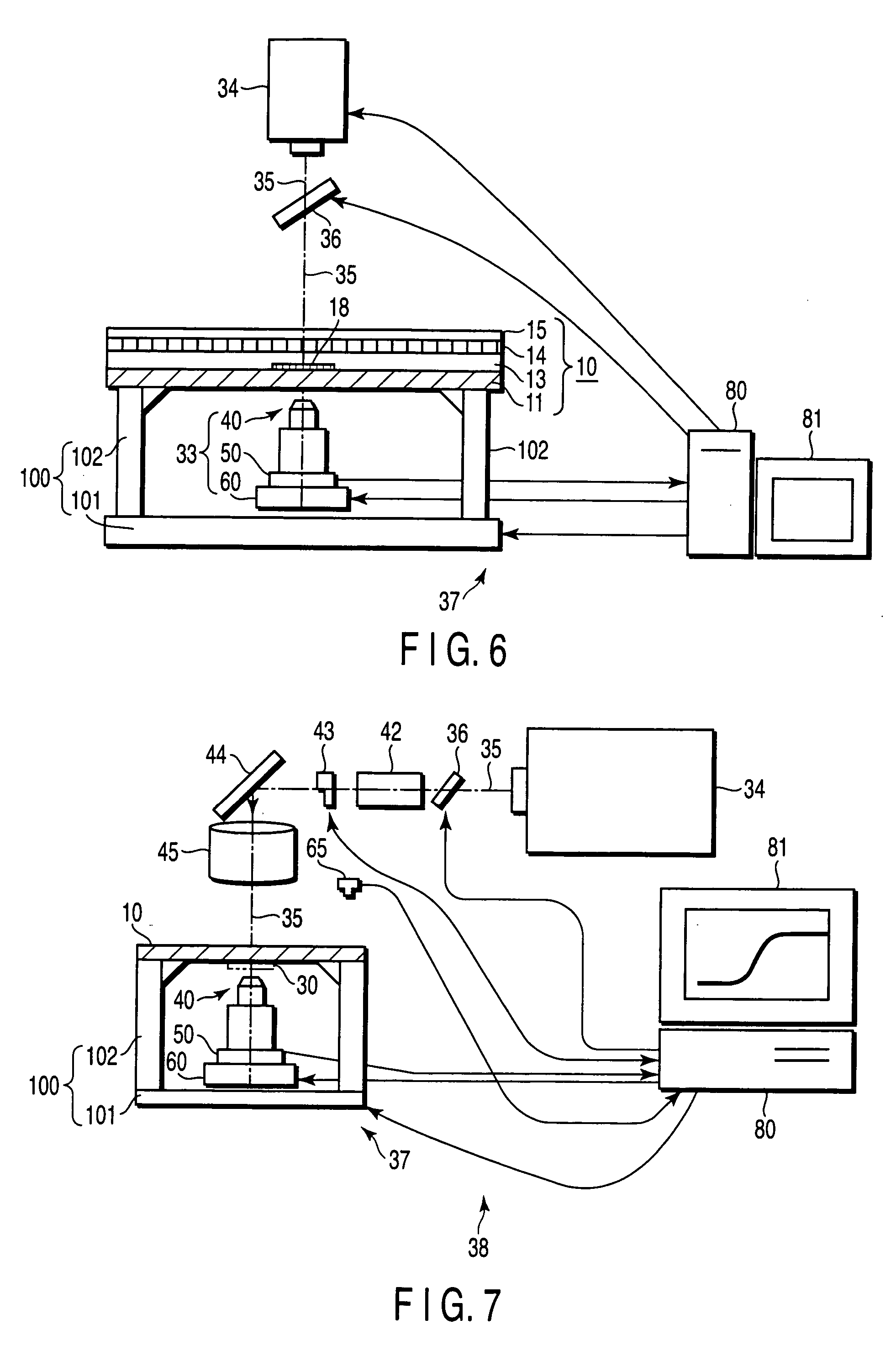
[0053]FIGS. 1A, 1B show an example of a substrate to be treated for laser annealing, having a non-single crystal semiconductor thin film and a light-emitting layer. In this example, the light intensity distribution can be imaged even in any position of the substrate to be treated.

[0054]FIG. 1A is a plan view of the substrate to be treated. In this example, a substrate 10 to be treated is a substrate for a liquid crystal display device, and has a square shape. A light-emitting layer 12 is formed on the whole flat face of the substrate 10 to be treated. FIG. 1B is a sectional view along line A-B of the substrate 10 to be treated of FIG. 1A. A substrate is a visible light transmitting substrate 11, for example, a general-purpose glass substrate. The light-emitting layer 12 which receives laser light to emit the light is formed (e.g., by coating) on the substrate 11. Furthermore, an underlayer insulating...

example 2

A Substrate to be Treated, on Whose Whole Surface a Light-Emitting Layer is Formed

[0059]FIG. 2 shows a sectional view of another example of a substrate to be treated for laser annealing, having a light-emitting layer. It is to be noted that a plan view is common to FIG. 1A described above. In the substrate to be treated shown in this example, the light-emitting layer is disposed on an upper-layer side of an amorphous semiconductor layer. The same part as that of FIG. 1B is denoted with the same reference numerals, and detailed description thereof is omitted.

[0060]FIG. 2 is a sectional view of the substrate to be treated of a portion corresponding to a line A-B in FIG. 1A. For example, an underlayer insulating film 13 (e.g., SiO2 layer) is formed on a substrate 11 formed of a general-purpose glass. An amorphous silicon layer 14 is formed as a non-single crystal semiconductor thin film on the underlayer insulating film 13. A cap film 15 (e.g., SiO2 layer) having a heat accumulating ...

example 3

A Substrate to be Treated on Which a Light-Emitting Layer is Partially Formed

[0063]FIGS. 3A, 3B show an example of a substrate to be treated for laser annealing, on which a light-emitting layer is partially disposed. The same part as that of FIGS. 1A, 1B is denoted with the same reference numerals, and detailed description thereof is omitted. The light-emitting layer is disposed in a striped form on the substrate to be treated in this example. In this example, since an area for forming the light-emitting layer is small, a use amount of a light-emitting material may be small.

[0064]FIG. 3A is a plan view of the substrate to be treated. In a substrate 10 to be treated, light-emitting layer regions 16 are formed in a striped form, and non-light-emitting layer regions 17 are formed in other regions. A size of the light-emitting layer region 16 is determined in accordance with a size of an imaging face. For example, when the imaging face has a diameter of about 100 μmφ, the size of the ...


PUM

PropertyMeasurementUnit
Thicknessaaaaaaaaaa
Thicknessaaaaaaaaaa
Lengthaaaaaaaaaa

Abstract

An amorphous silicon layer is deposited on a glass substrate via an underlayer insulating film, and further a light-emitting layer is inserted between the glass substrate and the underlayer insulating film in a partial region on the glass substrate. To measure light intensity distribution of laser light applied to the amorphous silicon layer, the laser light is applied to the light-emitting layer from the surface of a substrate to be treated. The light intensity distribution of the light emitted from the light-emitting layer is two-dimensionally imaged using an optical image pickup system from the back surface of the substrate to be treated, and measured using an image pickup device. The light intensity distribution of the laser light in the face to be treated is obtained from the light intensity distribution of the emission measured in this manner.

Description

CROSS-REFERENCE TO RELATED APPLICATIONS [0001] This application is based upon and claims the benefit of priority from prior Japanese Patent Application No. 2004-280708, filed Sep. 27, 2004, the entire contents of which are incorporated herein by reference. BACKGROUND OF THE INVENTION [0002] 1. Field of the Invention [0003] The present invention relates to a method of measuring an intensity distribution of laser light applied to a semiconductor device, and a semiconductor device to which this method is applied. The method of the present invention is suitable especially for measurement of the intensity distribution of ultraviolet laser light for use in laser-annealing a semiconductor thin film. Furthermore, the present invention relates to a laser annealing apparatus in which an image pickup device for measuring a laser light intensity distribution using the above-described method is incorporated, and a crystallization method in which the above-described method is used. [0004] 2. Desc...

Claims


Application Information

Patent Timeline
IPC IPC(8): B23K26/00H01L21/268
CPCB23K26/422H01L21/2026G01J1/58G01J1/429B23K26/702H01L21/02686H01L21/02488H01L21/02502H01L21/02678H01L21/02422H01L21/02532H01L21/02675
Inventor JYUMONJI, MASAYUKIHIRAMATSU, MASATOMATSUMURA, MASAKIYO
Owner ADVANCED LCD TECH DEVMENT CENT
Why Eureka
Try Eureka