Methods for forming and patterning of metallic films

a technology of metallic film and patterning, which is applied in the direction of thermoplastic polymer dielectrics, printing, spray discharge apparatus, etc., can solve the problems of insufficient adhesion of metal pattern to substrate, easy to come off, and complicated fabrication process, etc., to achieve simplification of manufacturing process, sufficient adhesion, and the effect of good adhesion

Inactive Publication Date: 2006-03-30
EBARA CORP
View PDF11 Cites 45 Cited by
  • Summary
  • Abstract
  • Description
  • Claims
  • Application Information

AI Technical Summary

Benefits of technology

[0013] The present invention has been devised in view of such circumstances, and an object of the present invention is to provide a wiring plating method that does not need the steps of application of a resist, lamination of a photosensitive dry film resist, exposure, etching of a copper foil and stripping of the photosensitive material that are essential for the conventional techniques to form a patterned plating wiring on a substrate, such as a printed circuit board, and assures sufficient adhesion of the obtained plating wiring to the substrate, thereby providing a technique that enables simplification of the manufacturing process and reduction of the manufacturing cost.

Problems solved by technology

However, these conventional fabrication processes for a printed circuit board all requires a series of steps including application of a photoresist, lamination of a photosensitive dry film resist, and stripping of the photoresist and the photosensitive dry film resist for patterning the plating wiring.
Thus, there is a problem that the fabrication processes are complicated.
Such a complication problem is not limited to the fabrication processes for a printed circuit board, but is found in a process of patterning a metal film on a silicon wafer, for example.
However, the study by the inventors has proved that the metal film patterned by the patterning method described in Japanese Patent Laid-Open No. 57-139923 is inferior in adhesion to the substrate, and the plating wiring on the printed circuit board patterned by this method cannot have a practically sufficient adhesion and is easy to come off.
In other words, while the patterning method described in Japanese Patent Laid-Open No. 57-139923 has an advantage that it can achieve highly sensitive patterning without using a resist, the resulting metal pattern does not adequately adhere to the substrate, and therefore, it is difficult to assure a high production yield of electronic components.
However, since the variety of metal elements that can be made into nanoparticles is limited, such a patterning technique has a problem that it is limited in application compared with a metal film patterning technique relying on plating.
In addition, there is a problem that, even if the metal element used is included in the limited variety of metal elements, if the sintering temperature is low, the electric resistance of the resulting pattern cannot be reduced adequately.

Method used


Image

  • Methods for forming and patterning of metallic films
  • Methods for forming and patterning of metallic films
  • Methods for forming and patterning of metallic films

Examples


embodiment 1

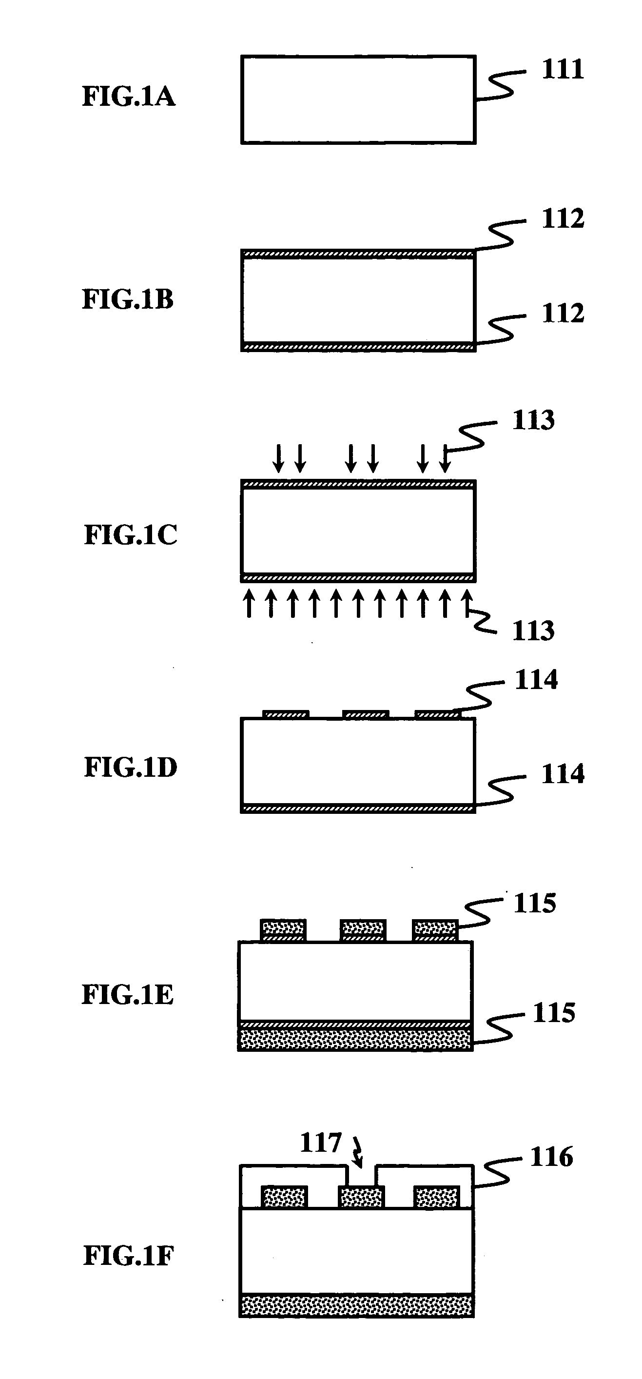
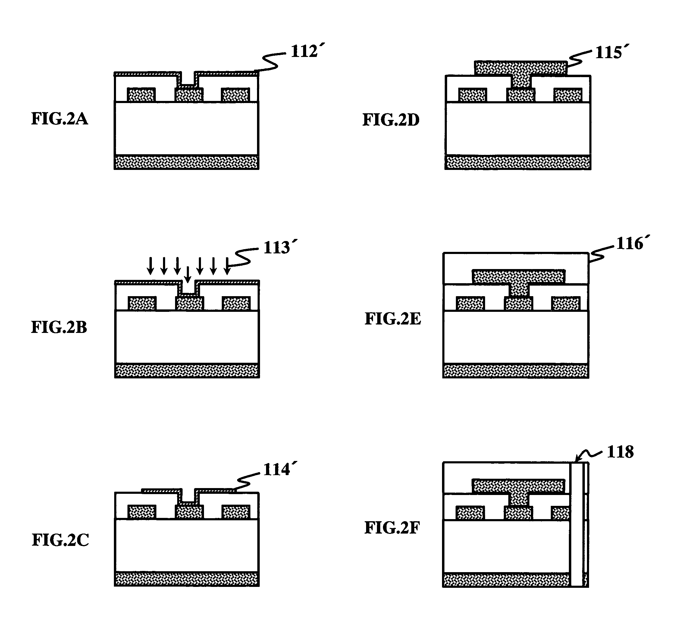
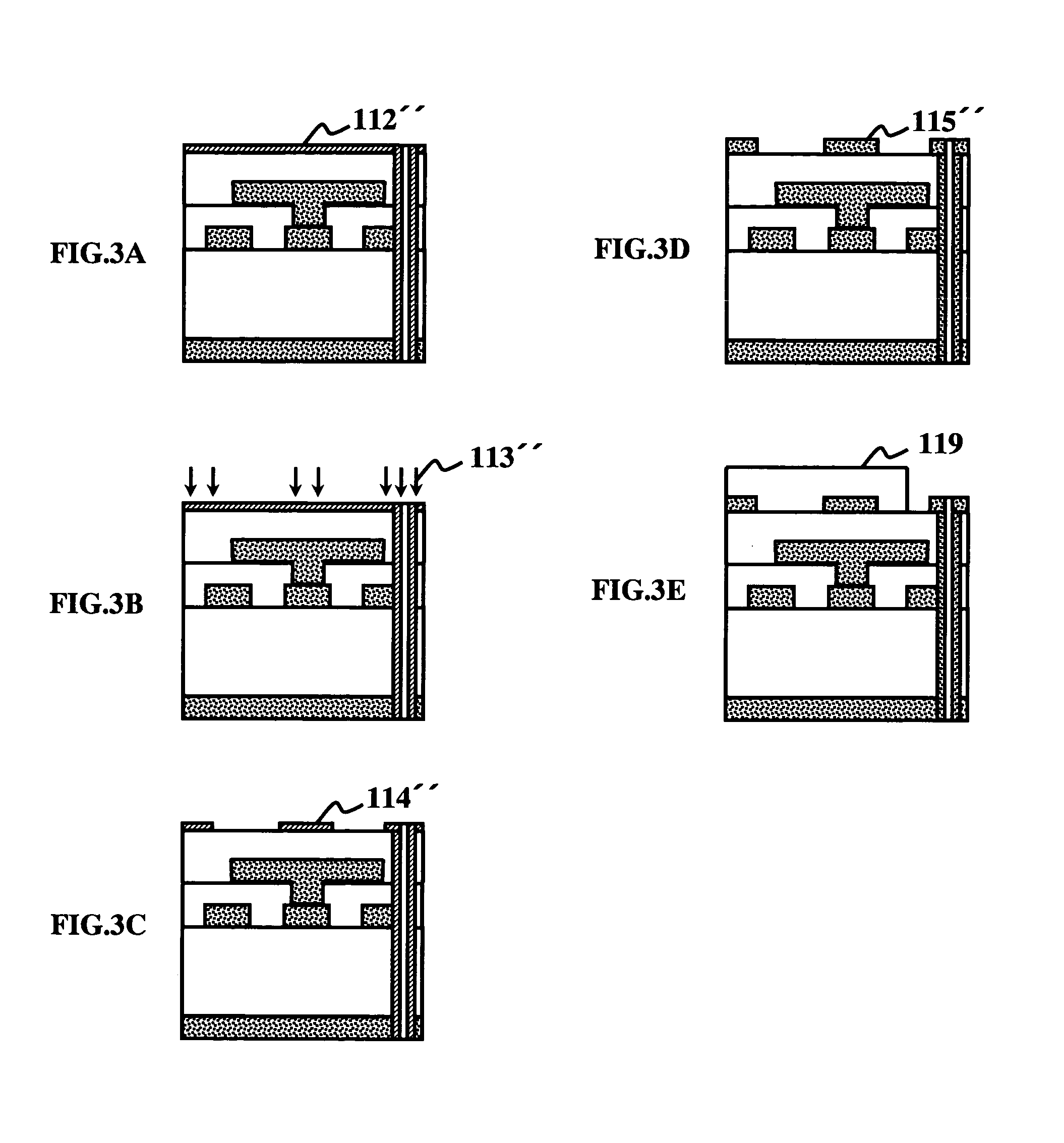
[0094]FIGS. 1A to 1F, FIGS. 2A to 2F, and FIGS. 3A to 3E are diagrams for illustrating a first example of a method of fabricating a printed circuit board according to the first aspect of the present invention, and the printed circuit board shown in these drawings for illustration has three layers of wiring pattern on one side. Here, FIGS. 1A to 1F, FIGS. 2A to 2F, and FIGS. 3A to 3E correspond to procedures of forming a wiring pattern of a first layer, a wiring pattern of a second layer and a wiring pattern of a third layer, respectively.

[0095] First, a substrate 111, which is an insulating planar substrate, is prepared (FIG. 1A), and a solvent containing an organic or inorganic metal compound containing a metal catalyst serving as a seed for plating is applied to the both principal surfaces of the substrate 111 and dried to form a metal compound film 112 (FIG. 1B). The substrate 111 used herein is a plastic substrate, which is a material whose surface area can be locally molten, a...

embodiment 2

[0105] An Embodiment 2 relates to a second example of the method of fabricating a printed circuit board according to the first aspect of the present invention and will be described with reference to FIGS. 1A to 1F, FIGS. 2A to 2F and FIGS. 3A to 3E, as in the embodiment 1. As described above, the printed circuit board shown in these drawings for illustration has three layers of wiring pattern on one side, and FIGS. 1A to 1F, FIGS. 2A to 2F and FIGS. 3A to 3E correspond to procedures of forming a wiring pattern of a first layer, a wiring pattern of a second layer and a wiring pattern of a third layer, respectively.

[0106] First, a substrate 111, which is an insulating planar substrate, is prepared (FIG. 1A), and a solvent containing an organic or inorganic metal compound containing a metal catalyst serving as a seed for plating is applied to the both principal surfaces of the substrate 111 and dried to form a metal compound film 112 (FIG. 1B). The substrate 111 used herein is aplasti...

embodiment 3

[0121] Referring to an embodiment 3, there will be described a first configuration of a patterning apparatus (a substrate fabricating apparatus) for fabricating a printed circuit board according to the first aspect of the present invention.

[0122]FIG. 4 is a conceptual diagram for illustrating the configuration of the patterning apparatus. A patterning apparatus 120 comprises at least a unit for forming a metal compound film, an energy beam irradiation unit, a washing unit for removing a metal compound film that has not been irradiated with the energy beam, a plating unit for plating a metal catalyst film formed by irradiation with the energy beam with a wiring-forming metal, a unit for applying an insulating film for surface protection and curing the insulating film, and a unit for forming a via hole or through hole.

[0123] The patterning apparatus 120 has a carrier unit for carrying a substrate (a printed circuit board, a silicon wafer or the like), which has a holding mechanism c...


PUM

PropertyMeasurementUnit
diameteraaaaaaaaaa
widthaaaaaaaaaa
diameteraaaaaaaaaa

Abstract

A solvent containing an organic or inorganic metal compound containing a metal catalyst that serves as a plating seed is applied to a plastic substrate and dried, thereby forming a metal compound film, and then, the metal compound film is irradiated with an energy beam, such as an electron beam, to precipitate the metal catalyst. By irradiating a local area of the metal compound film with the energy beam, the chemical reaction of metal catalyst precipitation can be caused locally in the irradiated area, and thus, a patterned metal catalyst film can be formed. Once the substrate is irradiated with the energy beam, the surface may be molten to trap the metal catalyst to an extremely shallow depth, so that the bonding between the substrate and the metal catalyst is enhanced. Thus, the metal catalyst film becomes harder to peel off the substrate.

Description

BACKGROUND OF THE INVENTION [0001] 1. Field of the Invention [0002] The present invention relates to a substrate having an insulating layer and a metallic film formed thereon, such as a printed circuit board and a silicon wafer, and a method of fabricating the same. More particularly, it relates to a technique of patterning or printing a metal catalyst film, which constitutes a seed for forming a metal plating layer, on an insulating layer of a printed circuit board or silicon wafer and plating the metal catalyst film. [0003] 2. Description of the Related Art [0004] Printed circuit boards, which are referred to also as printed wiring boards and fabricated by forming a conductive wiring pattern on an insulating substrate by plating or the like, provide a basis for circuit implementation. [0005] As methods of forming a circuit pattern on such a printed circuit board, for example, there are known an etching method using a photosensitive resist, a subtractive method involving plating a ...

Claims


Application Information

Patent Timeline
Patent Type & Authority Applications(United States)
IPC IPC(8): B32B15/04B41M5/00B05D1/36B05D1/18C23C16/00B05B5/025B21D39/00
CPCB05C3/10Y10T428/24802C23C18/30H05K3/185H05K3/387H05K2201/0129H05K2203/092H05K2203/107C23C18/1608C23C18/1612C23C18/165C23C18/2066C23C18/1692C23C18/206C25D7/123C25D17/001Y10T428/12556C23C18/14C23C18/143C23C18/145Y10T428/31678
Inventor KAJIYAMA, MASAAKIHORITA, OSAMU
Owner EBARA CORP
Why Eureka
Try Eureka