Protective tape separation method, and apparatus using the same

a protective tape and separation method technology, applied in the direction of layered products, solid-state devices, chemical apparatus and processes, etc., can solve the problems of low separation stability, difficult thickness adjustment, and conventional protective tape separation methods, and achieve high precision

Inactive Publication Date: 2006-03-30
NITTO DENKO CORP
View PDF7 Cites 23 Cited by
  • Summary
  • Abstract
  • Description
  • Claims
  • Application Information

AI Technical Summary

Benefits of technology

[0009] The invention has been achieved in view of the above circumstances, and a main object of the invention is to provide a protective tape separation method capable of joining an adhesive tape to a protective tape joined to the surface of a semiconducto...

Problems solved by technology

The conventional protective tape separation method, however, has the following problems.
Consequently, pressure on the adhesive tape Ts with a roller 60 is uneven due to the gap G. The adhesive tape Ts is not firmly made close-contact with the end of a protective tape PT particularly at the joining start end due to the gap G. It causes a problem in that separation stability is low at ...

Method used


Image

  • Protective tape separation method, and apparatus using the same
  • Protective tape separation method, and apparatus using the same
  • Protective tape separation method, and apparatus using the same

Examples


Embodiment Construction

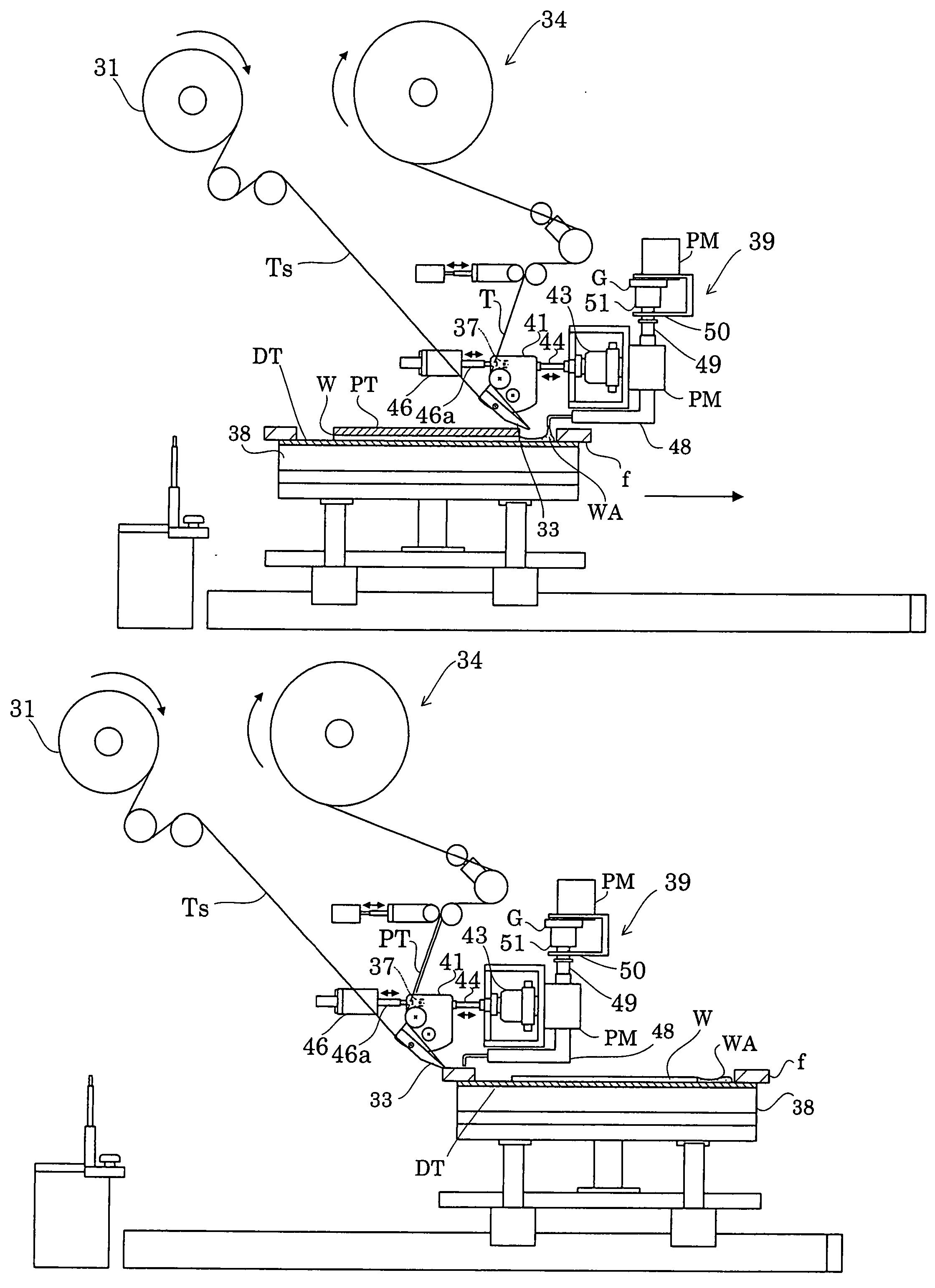
[0050] An embodiment of a semiconductor wafer mount apparatus provided with a protective tape separation apparatus of the invention will be described below with reference to the drawings.

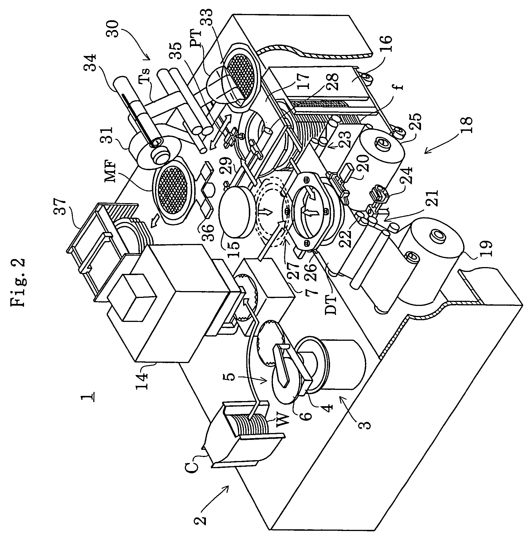
[0051]FIG. 2 is a cutaway perspective view illustrating a whole configuration of a semiconductor wafer mount apparatus according to an embodiment of the invention.

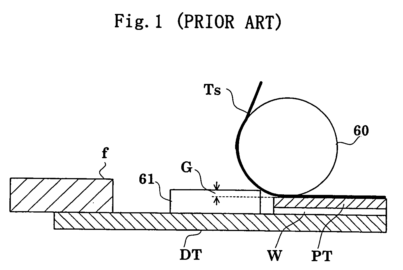
[0052] A semiconductor wafer mount apparatus 1 includes a wafer supply part 2 in which cassettes C for housing wafers W subjected to a back grinding process in multiple stages are loaded, a wafer transport mechanism 3 having a robot arm 4 and a pressing mechanism 5, an alignment stage 7 for aligning the wafer W, an ultraviolet irradiation unit 14 for emitting ultraviolet rays toward the wafer W mounted on the alignment stage 7, a chuck table 15 for suction-holding the wafer W, a ring frame supply part 16 in which ring-shaped frames (hereinafter, simply referred to as “ring frames f”) are housed in multiple stages, a ring frame transport ...


PUM

PropertyMeasurementUnit
Viscosityaaaaaaaaaa
Adhesion strengthaaaaaaaaaa

Abstract

The invention relates to an apparatus for separating a protective tape joined to a semiconductor wafer. Before joining a separation tape to a protective tape on a surface of a semiconductor wafer held, from its back side, by a ring frame via a dicing tape while pressing the separation tape against the protective tape with the use of an edge member, pure water is dropped from a piston nozzle onto the back side of the dicing tape located in front of a joining start end of the separation tape.

Description

BACKGROUND OF THE INVENTION [0001] (1) Field of the Invention [0002] The invention relates to a protective tape separation method capable of joining an adhesive tape to a protective tape joined to the surface of a semiconductor wafer held by a ring-shaped frame via a supporting adhesive tape and separating the protective tape integrally with the adhesive tape from the semiconductor wafer with high precision, and to an apparatus using the same. [0003] (2) Description of the Related Art [0004] A semiconductor wafer (hereinafter, simply referred to as “wafer”) is thinned by processing the back side of the wafer by using a mechanical method such as grinding or polishing or a chemical method using etching. At the time of processing the wafer by using any of the methods, a protective tape is joined to the surface of the wafer to protect the surface on which a wiring pattern is formed. The back side of the wafer to which the protective tape is joined and which is polished is suction-held b...

Claims


Application Information

Patent Timeline
IPC IPC(8): H01L21/50H01L21/48H01L21/44
CPCB29C63/0013H01L21/67132H01L21/6835H01L21/6836Y10T156/1111H01L2221/6834H01L2221/6839Y10T156/16H01L2221/68327H01L21/02H01L21/304
Inventor YAMAMOTO, MASAYUKI
Owner NITTO DENKO CORP
Why Eureka
Try Eureka