Output buffer circuit and semiconductor device

a buffer circuit and output terminal technology, applied in logic circuit coupling/interface arrangement, digital transmission, pulse technique, etc., can solve the problems of delay in timing and production of jitter, and achieve the effect of reducing jitter, suppressing the increase of capacitance across output terminals, and reducing jitter

Inactive Publication Date: 2006-04-06
RENESAS ELECTRONICS CORP
View PDF4 Cites 11 Cited by
  • Summary
  • Abstract
  • Description
  • Claims
  • Application Information

AI Technical Summary

Benefits of technology

[0027] According to the present invention, capacitance coupling is produced in the output buffer circuit having the pre-emphasis function, when the output signal is changed, thereby reducing the jitter. Moreover, according to the present invention, techniques in capacitance coupling, exploiting the cross-talk, may be employed to reduce the jitter as the capacitance across the output terminals is suppressed from increasing.

Problems solved by technology

This difference, that is, whether the pre-emphasis directly before change in the logic signal is on or off, results in the difference in voltage of a start point directly before change in the logic signal, thus possibly producing the jitter.
For example, if, when the output signal SOUT of FIG. 11 is changed from a low level to a high level, the pre-emphasis is off directly before such change, it is sufficient for the signal SOUT to start from Vol2, whereas, if the pre-emphasis is on directly before such change, the signal SOUT has to start from Vol1, meaning a handicapped start, thus naturally causing delay in the timing until rise of the signal SOUT.

Method used


Image

  • Output buffer circuit and semiconductor device
  • Output buffer circuit and semiconductor device
  • Output buffer circuit and semiconductor device

Examples


Embodiment Construction

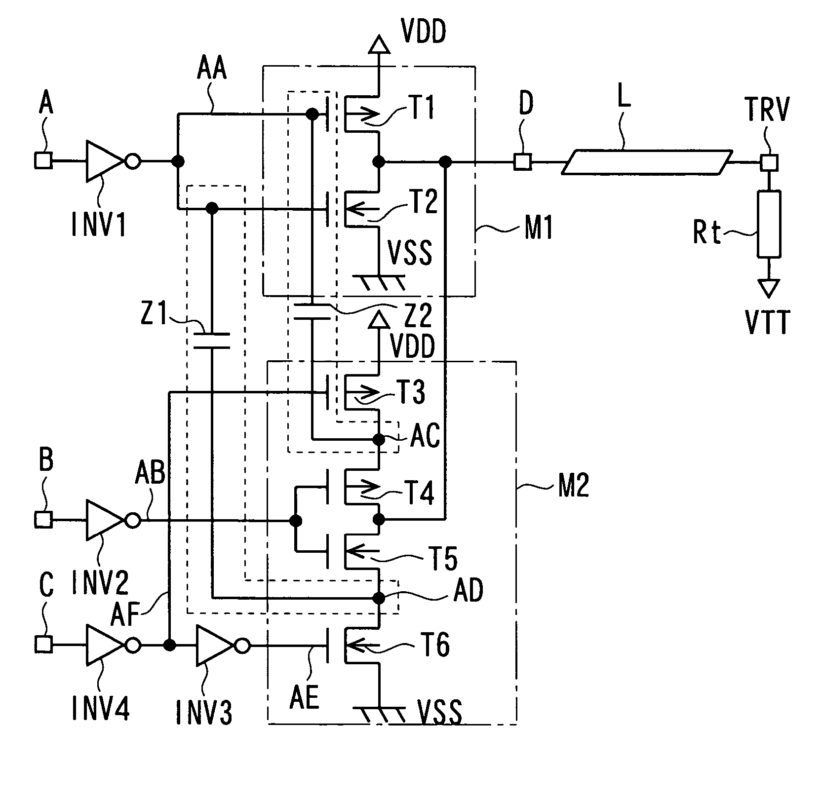
[0047] Preferred embodiments of the present invention will now be described. According to the present invention, capacitance coupling is produced when the output signal is changed, in an output (I / O) circuit of a semiconductor integrated circuit, thereby reducing jitter at the time of high-speed transmission. The output (I / O) circuit is provided with the pre-emphasis function, that is, the function of emphasizing the amplitude of a transmission signal on the transmitting side when the signal is changed, in order to prevent pattern-dependent deterioration of the transmission signal, thereby improving the waveform on the receiving end.

[0048] An output buffer circuit, in one mode for practicing the present invention, includes a first buffer circuit (M1) (inverting buffer circuits (T1, T2)), receiving a first logic signal to drive the transmission line (L), and a second buffer circuit (M2). The second buffer circuit (M2) includes an inverting buffer (T4, T5), a first switch (T3), a sec...


PUM


Abstract

Disclosed is an output buffer circuit provided with a pre-emphasis function, including a first buffer circuit, receiving a first logic signal to drive a transmission line, and a second buffer circuit. The second buffer circuit includes an inverting buffer, receiving a second logic signal that is in a predetermined logical relationship with respect to the aforementioned first logic signal, and having outputs connected in common with an output of the aforementioned first buffer circuit, a first switch, connected across the inverting buffer and a first power supply, and controlled to be turned on or off based on a signal supplied to a control terminal, and a second switch, connected across the inverting buffer and a second power supply and controlled to be turned on or off based on a signal supplied to a control terminal in association operatively with the first switch. The output buffer circuit also includes first and second capacitors across an input end of the first buffer circuit and a connection node between the inverting buffer and the first switch and across the input end of the first buffer circuit and a connection node between the inverting buffer and the second switch.

Description

FIELD OF THE INVENTION [0001] This invention relates to an output buffer circuit of a semiconductor device and, more particularly, to an output buffer circuit having a pre-emphasis function. BACKGROUND OF THE INVENTION [0002] With the advent of the broadband technique and high-speed transmission rate in recent years, deterioration in the transmission waveform in serial signal transmission has become of a serious problem. The function of pre-emphasis is a technique of emphasizing the amplitude of a transmission signal at the time of transition thereof on a transmission side, in order to prevent pattern-dependent deterioration of the transmission signal, thereby improving a waveform of the signal on a receiving side. In the transmission at the rate on the order of GHz, in which the log of signal attenuation due to skin effect and dielectric losses per unit distance of a transmission line increases in proportion to the log of the frequency of signal, the application of pre-emphasis is ...

Claims


Application Information

Patent Timeline
Patent Type & Authority Applications(United States)
IPC IPC(8): H03K19/0175
CPCH04L25/0272
Inventor UENISHI, YASUTAKA
Owner RENESAS ELECTRONICS CORP
Why Eureka
Try Eureka