Group III-nitride based HEMT device with insulating GaN/AlGaN buffer layer

a technology of hemt devices and buffer layers, applied in the direction of semiconductor devices, basic electric elements, electrical equipment, etc., can solve the problems of affecting the performance of the device, the background impurity concentration of mbe-grown gallium nitride can be substantially low, and the growth technique is very slow

Inactive Publication Date: 2006-04-06
PALO ALTO RES CENT INC
View PDF19 Cites 93 Cited by
  • Summary
  • Abstract
  • Description
  • Claims
  • Application Information

AI Technical Summary

Problems solved by technology

Unfortunately, MBE is a very slow growth technique.
The background impurity concentrations for MBE-grown gallium nitride can be substantially low, accordingly, gallium nitride films grown via MBE are generally expected to be sufficiently insulating for most high speed device applications, but the nucleation layer underneath the gallium nitride layer is generally conducting and has a negative impact on the performance of the device.
Moreover, because MBE is a slow growth technique, it is not suitable for mass production.
A conductive gallium nitride buffer layer results in parasitic capacitances, which are detrimental to high speed operation of gallium nitride based HEMT devices.

Method used


Image

  • Group III-nitride based HEMT device with insulating GaN/AlGaN buffer layer
  • Group III-nitride based HEMT device with insulating GaN/AlGaN buffer layer
  • Group III-nitride based HEMT device with insulating GaN/AlGaN buffer layer

Examples


Embodiment Construction

[0023] These and other features and advantages of this invention are described in, or are apparent from, the following detailed description of various exemplary embodiments of the systems and methods according to this invention.

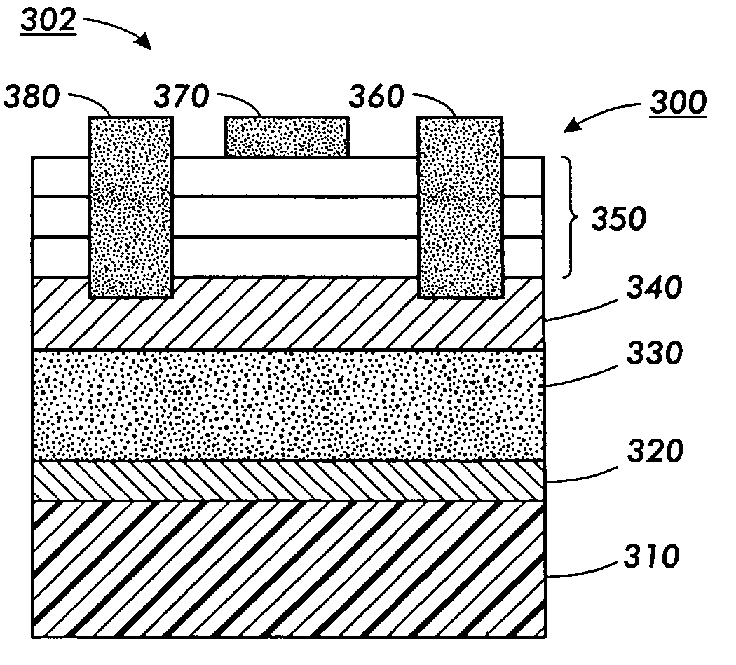
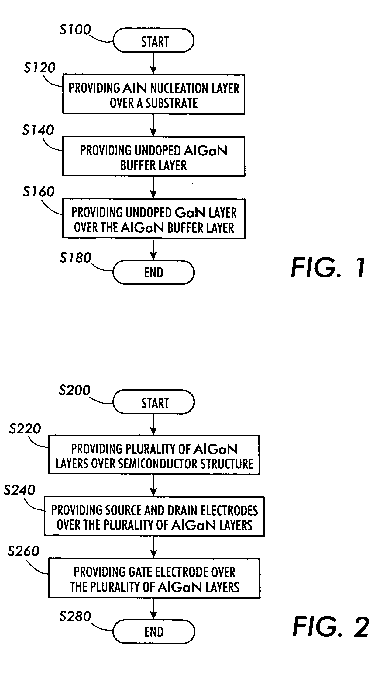
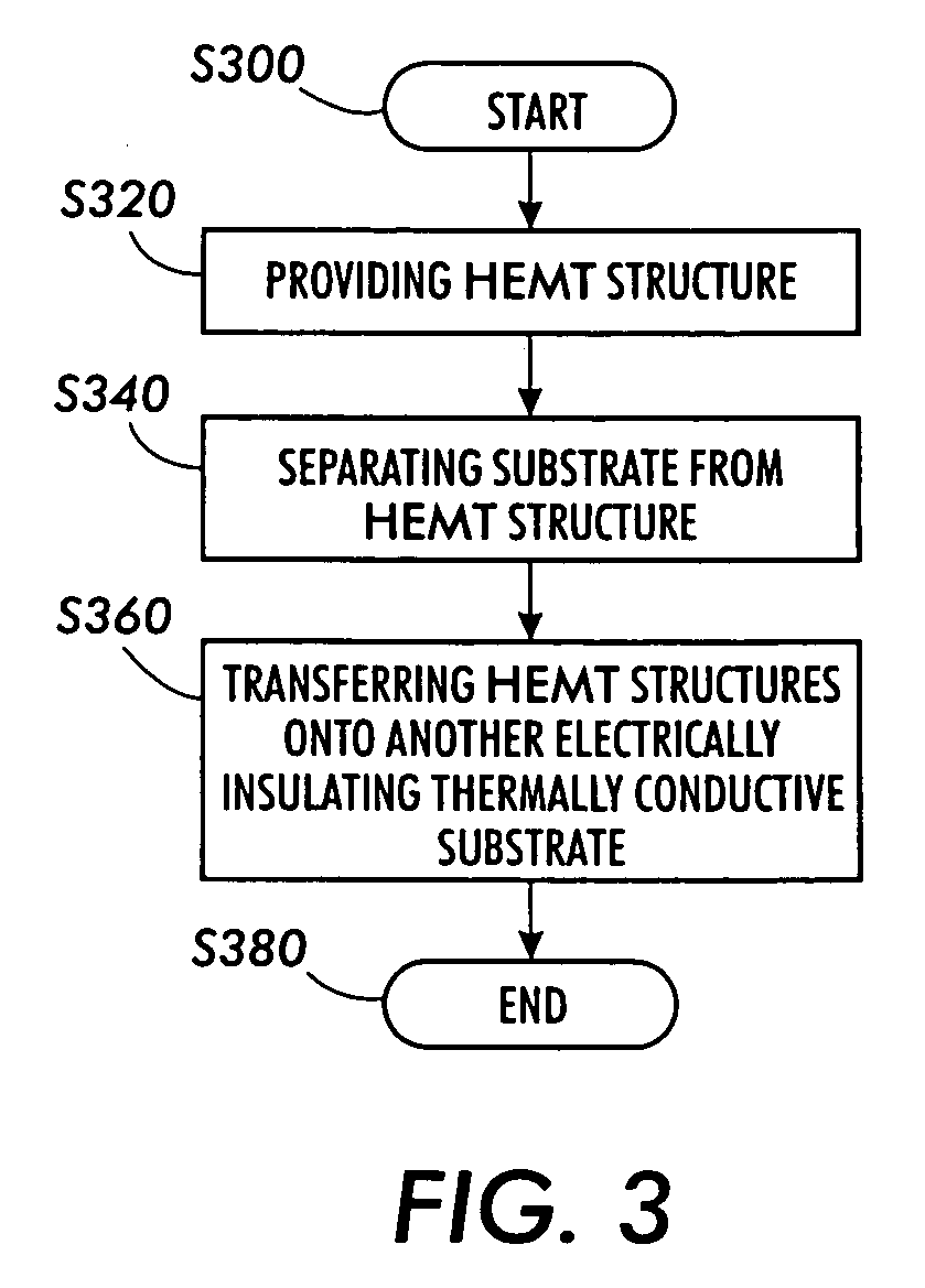
[0024]FIG. 1 is a flowchart illustrating a method of manufacturing a layered aluminum nitride (AlN) and aluminum gallium nitride (AlGaN) structure according to various exemplary embodiments of this invention. The method starts in step S100 and continues to step S120, during which an AlN nucleation layer is provided over a substrate. According to various exemplary embodiments of this invention, the substrate can be sapphire, aluminum nitride (AlN), gallium nitride (GaN), silicon carbide (SiC), or silicon (Si). According to various exemplary embodiments, when an AlN or GaN substrate is used, it might not be necessary to provide an AlN nucleation layer. Instead, MOCVD growth can be initiated by immediately providing the AlGaN buffer layer without the AlN buffer...


PUM

PropertyMeasurementUnit
thicknessaaaaaaaaaa
thicknessaaaaaaaaaa
thicknessaaaaaaaaaa

Abstract

Various exemplary embodiments of the devices and methods for this invention provide for a semiconductor structure and a method of manufacturing a semiconductor structure that includes providing an aluminum nitride nucleation layer over a substrate, providing an undoped AlGaN buffer layer over the aluminum nitride nucleation layer, providing an undoped GaN over the AlGaN buffer layer, providing a plurality of AlGaN layers over the GaN layer wherein the plurality of aluminum GaN layers comprise a first layer provided over the undoped GaN layer, a second layer provided over the first layer and the third layer provided over the second layer, providing a source electrode and a drain electrode, through the first, second and third aluminum gallium nitride layers, the source electrode and the drain electrode being in electrical contact with the gallium nitride layer and providing a gate electrode over the third aluminum gallium nitride layer.

Description

BACKGROUND OF THE INVENTION [0001] 1. Field of Invention [0002] This invention relates to transistor devices and in particular relates to nucleation layers in the transistor devices. [0003] 2. Description of Related Art [0004] Gallium nitride based high electron mobility transistors (HEMTs) are very attractive electronic devices because of their high breakdown fields, high temperature stability and high power, high frequency handling capability. HEMTs may be used for a variety of applications such as, cell phone base stations or automobile electronics. Currently, most gallium nitride HEMTs are grown by molecular beam epitaxy (MBE) because HEMT devices require an insulating buffer layer for high speed operation. Unfortunately, MBE is a very slow growth technique. [0005] The background impurity concentrations for MBE-grown gallium nitride can be substantially low, accordingly, gallium nitride films grown via MBE are generally expected to be sufficiently insulating for most high speed ...

Claims


Application Information

Patent Timeline
Patent Type & Authority Applications(United States)
IPC IPC(8): H01L21/00
CPCH01L29/2003H01L29/66462H01L29/7785H01L29/7787
Inventor KNEISSEL, MICHAEL A.KIESEL, PETERWONG, WILLIAMTREAT, DAVID W.
Owner PALO ALTO RES CENT INC
Why Eureka
Try Eureka